AD2.5V to 5.5V, 400μA Quad Voltage Output, 8-10-12-Bit DACs in 16-Lead TSSOP AD5307 AD5317 AD5327 Data Sheet Manual User Guide
Summary
These advanced quad DAC chips provide high-resolution (8 to 12-bit) voltage outputs for demanding applications, including industrial control and portable instrumentation. Optimized for low power consumption (down to 90 nA), they integrate versatile serial interfaces compatible with SPI, QSPI, MICROWIRE, and DSP standards. The accompanying documentation details comprehensive features such as double-buffered references, rail-to-rail output amplifiers, and daisy-chaining. This resource is essential for engineers designing reliable signal generation circuits requiring customizable voltage range and resolution.
Page 1 Text Content
2.5 V to 5.5 V, 400 μA, Quad Voltage Output, 8-/10-/12-Bit DACs in 16-Lead TSSOP
AD5307/AD5317/AD5327 FEATURES GENERAL DESCRIPTION AD5307: 4 buffered 8-bit DACs in 16-lead TSSOP
The AD5307/AD5317/AD53271 are quad 8-,10-,12-bit buffered
A version: ±1 LSB INL; B version: ±0.625 LSB INL
voltage-output DACs in 16-lead TSSOP that operate from single
AD5317: 4 buffered 10-bit DACs in 16-lead TSSOP
2.5 V to 5.5 V supplies and consume 400 μA at 3 V. Their on-
A version: ±4 LSB INL; B version: ±2.5 LSB INL
AD5327: 4 buffered 12-bit DACs in 16-lead TSSOP chip output amplifiers allow the outputs to swing rail-to-rail with A version: ±16 LSB INL; B version: ±10 LSB INL a slew rate of 0.7 V/μs. The AD5307/AD5317/AD5327 utilize Low power operation: 400 μA @ 3 V, 500 μA @ 5 V versatile 3-wire serial interfaces that operate at clock rates up to
2.5 V to 5.5 V power supply 30 MHz; these parts are compatible with standard SPI, QSPI, Guaranteed monotonic by design over all codes MICROWIRE, and DSP interface standards. Power down to 90 n A @ 3 V, 300 n A @ 5 V (LDAC pin)
The references for the four DACs are derived from two reference
Double-buffered input logic
Buffered/unbuffered reference input options pins (one per DAC pair). These reference inputs can be configured Output range: 0 V to VREF or 0 V to 2 VREF as buffered or unbuffered inputs. Each part incorporates a power- Power-on reset to 0 V on reset circuit, ensuring that the DAC outputs power up to 0 V Simultaneous update of outputs (LDAC pin) and remain there until a valid write to the device takes place.
Asynchronous clear facility (CLR pin) There is also an asynchronous active low CLR pin that clears all Low power, SPI®-, QSPI™-, MICROWIRE™-, and DSP- DACs to 0 V. The outputs of all DACs can be updated simul- compatible 3-wire serial interface
taneously using the asynchronous LDAC input. Each part
SDO daisy-chaining option
contains a power-down feature that reduces the current
On-chip rail-to-rail output buffer amplifiers
consumption of the device to 300 n A @ 5 V (90 n A @ 3 V). The
Temperature range of −40°C to +105°C
parts can also be used in daisy-chaining applications using the
APPLICATIONS
SDO pin.
Portable battery-powered instruments
Digital gain and offset adjustment All three parts are offered in the same pinout, allowing users to
Programmable voltage and current sources select the amount of resolution appropriate for their application Programmable attenuators without redesigning their circuit board.
Industrial process control
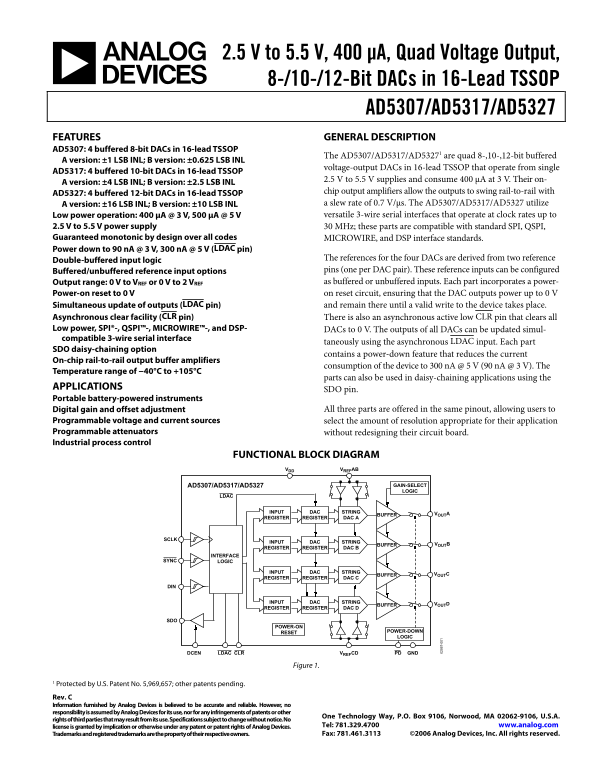
FUNCTIONAL BLOCK DIAGRAM
VDD VREFAB
AD5307/AD5317/AD5327 GAIN-SELECT LOGIC
INPUT DAC STRING VOUTA
BUFFER
REGISTER REGISTER DAC A
INPUT DAC STRING
BUFFER VOUTB
REGISTER REGISTER DAC B
INTERFACE
SYNC LOGIC
INPUT DAC STRING VOUTC
BUFFER
REGISTER REGISTER DAC C
INPUT DAC STRING VOUTD
BUFFER
REGISTER REGISTER DAC D
POWER-ON
RESET POWER-DOWN LOGIC
CLRDCEN VREFCD PDLDAC GND
Figure 1.
1 Protected by U.S. Patent No. 5,969,657; other patents pending.
Rev. C Information furnished by Analog Devices is believed to be accurate and reliable. However, no responsibility is assumed by Analog Devices for its use, nor for any infringements of patents or other
One Technology Way, P.O. Box 9106, Norwood, MA 02062-9106, U.S.A.
rights of third parties that may result from its use. Specifications subject to change without notice. No
license is granted by implication or otherwise under any patent or patent rights of Analog Devices. Tel: 781.329.4700 www.analog.com Trademarks and registered trademarks are the property of their respective owners. Fax: 781.461.3113 ©2006 Analog Devices, Inc. All rights reserved.
Page Summary Contents For AD2.5V to 5.5V, 400μA Quad Voltage Output, 8-10-12-Bit DACs in 16-Lead TSSOP AD5307 AD5317 AD5327 Data Sheet Manual User Guide
Manual Details
| Brand | QUAD |
|---|---|
| Pages | 28 |
| File Size | 578.72 KB |
| Published | June 04, 2026 |
Enter the captcha to get the download link:

Frequently Asked Questions
What serial interfaces are supported by these DACs?
They support standard SPI, QSPI, MICROWIRE, and DSP interface standards.
What is the typical maximum operating voltage and lowest standby power consumption?
The parts operate from a 2.5 V to 5.5 V supply and can enter a low-power state down to 90 nA @ 3 V.
How can I clear all four DAC outputs simultaneously?
You can use the asynchronous active low CLR pin, which clears all DACs to 0 V.
Can multiple AD5307/AD5317 chips be connected together?
Yes, they support daisy-chaining applications using the SDO pin.