MAXIM MAX5187 MAX5190 8-Bit, 40MHz, Current Voltage-Output DACs
Summary
Discover high-performance signal integrity with the MAX5187/MAX5190 DACs. These 8-bit, current/voltage output converters are ideal for demanding applications like arbitrary waveform generation and signal reconstruction. Designed for single-supply operation (+2.7V to +3.3V), they deliver low distortion and a wide spurious-free dynamic range (up to 70dB). The manual provides comprehensive details on performance metrics, advanced power-saving modes, and proper PCB design guidelines for optimal integration in your digital signal processing projects.
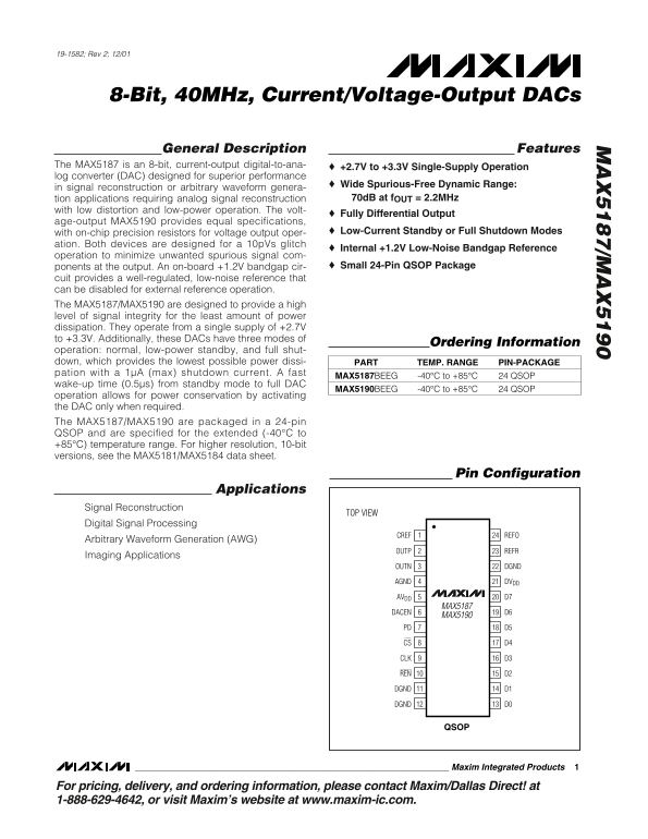
Page 1 Text Content
19-1582; Rev 2; 12/01
8-Bit, 40MHz, Current/Voltage-Output DACs
General Description Features
The MAX5187 is an 8-bit, current-output digital-to-ana- +2.7V to +3.3V Single-Supply Operation log converter (DAC) designed for superior performance
Wide Spurious-Free Dynamic Range:
in signal reconstruction or arbitrary waveform genera-
tion applications requiring analog signal reconstruction 70d B at f OUT = 2.2MHz
with low distortion and low-power operation. The volt-
Fully Differential Output
age-output MAX5190 provides equal specifications,
with on-chip precision resistors for voltage output oper- Low-Current Standby or Full Shutdown Modes
ation. Both devices are designed for a 10p Vs glitch
Internal +1.2V Low-Noise Bandgap Reference
operation to minimize unwanted spurious signal com-
ponents at the output. An on-board +1.2V bandgap cir- Small 24-Pin QSOP Package
cuit provides a well-regulated, low-noise reference that can be disabled for external reference operation. The MAX5187/MAX5190 are designed to provide a high level of signal integrity for the least amount of power dissipation. They operate from a single supply of +2.7V to +3.3V. Additionally, these DACs have three modes of
Ordering Information
operation: normal, low-power standby, and full shut- down, which provides the lowest possible power dissi- PART TEMP. RANGE PIN-PACKAGE pation with a 1µA (max) shutdown current. A fast
MAX5187BEEG -40°C to +85°C 24 QSOP
wake-up time (0.5µs) from standby mode to full DAC
MAX5190BEEG -40°C to +85°C 24 QSOP
operation allows for power conservation by activating the DAC only when required. The MAX5187/MAX5190 are packaged in a 24-pin QSOP and are specified for the extended (-40°C to +85°C) temperature range. For higher resolution, 10-bit versions, see the MAX5181/MAX5184 data sheet.
Pin Configuration
Applications
Signal Reconstruction
TOP VIEW
Digital Signal Processing
CREF REFO
Arbitrary Waveform Generation (AWG)
OUTP REFR
Imaging Applications
OUTN DGND
AGND DVDD
AVDD D7
MAX5187
DACEN D6
MAX5190
PD D5
CS D4
CLK D3
REN D2
DGND D1
D0DGND
Maxim Integrated Products
For pricing, delivery, and ordering information, please contact Maxim/Dallas Direct! at 1-888-629-4642, or visit Maxim’s website at www.maxim-ic.com.
Page Summary Contents For MAXIM MAX5187 MAX5190 8-Bit, 40MHz, Current Voltage-Output DACs
Manual Details
| Brand | Current |
|---|---|
| Pages | 15 |
| File Size | 278.93 KB |
| Published | May 28, 2026 |
Enter the captcha to get the download link:

Frequently Asked Questions
What operational temperature range do the DACs support?
The MAX5187/MAX5190 are specified for the extended temperature range of -40°C to +85°C.
Can I run this device on a single supply voltage?
Yes, the devices operate from a single supply of +2.7V to +3.3V.
How do I ensure optimal signal integrity for high speeds?
Use a multilayer PCB with separate analog and digital ground planes, and decouple AV/DV pins using 10µF and 0.1µF capacitors.
What are the modes of operation for power saving?
The DACs offer three modes: normal use, low-power standby, and full shut-down (with a minimal shutdown current of 1µA max).
Which MAX series device offers voltage output capability?
The MAX5190 provides equal specifications to the MAX5187 but is explicitly mentioned for voltage output operation.