MAXIM MAX5853 Dual, 10-Bit, 80 Msps, Current-Output DAC User Manual and Data Sheet
Summary
This dual, 10-bit, 80Msps Digital-to-Analog Converter (DAC) provides superior dynamic performance for critical wideband communication links. Engineered for low power consumption and robust operation from a single voltage supply (2.7V–3.6V), it features programmable channel gain matching and an integrated low-noise reference. The device is designed for sophisticated wireless systems, including SatCom, WLAN, HFC, and applications requiring precise quadrature modulation. This manual provides comprehensive details on its technical specifications, operating modes, performance metrics, and packaging options for engineers designing high-fidelity base stations and communication equipment.
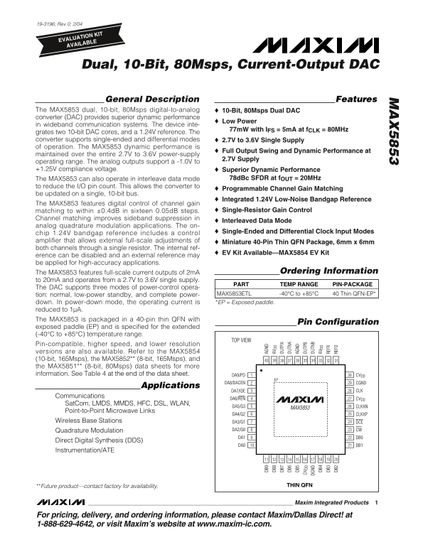
Page 1 Text Content
19-3196; Rev 0; 2/04
EVALUATION KIT AVAILABLE
Dual, 10-Bit, 80Msps, Current-Output DAC
General Description Features
The MAX5853 dual, 10-bit, 80Msps digital-to-analog 10-Bit, 80Msps Dual DAC converter (DAC) provides superior dynamic performance
Low Power
in wideband communication systems. The device inte-
77m W with IFS = 5m A at f CLK = 80MHz
grates two 10-bit DAC cores, and a 1.24V reference. The converter supports single-ended and differential modes 2.7V to 3.6V Single Supply of operation. The MAX5853 dynamic performance is
Full Output Swing and Dynamic Performance at
maintained over the entire 2.7V to 3.6V power-supply
2.7V Supply
operating range. The analog outputs support a -1.0V to +1.25V compliance voltage. Superior Dynamic Performance
The MAX5853 can also operate in interleave data mode 78d Bc SFDR at f OUT = 20MHz
to reduce the I/O pin count. This allows the converter to
Programmable Channel Gain Matching
be updated on a single, 10-bit bus.
Integrated 1.24V Low-Noise Bandgap Reference
The MAX5853 features digital control of channel gain
matching to within ±0.4d B in sixteen 0.05d B steps. Single-Resistor Gain Control
Channel matching improves sideband suppression in
Interleaved Data Mode
analog quadrature modulation applications. The on-
Single-Ended and Differential Clock Input Modes
chip 1.24V bandgap reference includes a control amplifier that allows external full-scale adjustments of
Miniature 40-Pin Thin QFN Package, 6mm x 6mm
both channels through a single resistor. The internal ref-
EV Kit Available—MAX5854 EV Kit
erence can be disabled and an external reference may be applied for high-accuracy applications.
DB AG ND
The MAX5853 features full-scale current outputs of 2m A Ordering Information
DB AV DD
to 20m A and operates from a 2.7V to 3.6V single supply. DB OU TP
PART TEMP RANGE PIN-PACKAGE
The DAC supports three modes of power-control opera-
DB OU TN
tion: normal, low-power standby, and complete power- MAX5853ETL -40°C to +85°C 40 Thin QFN-EP*
AG ND
down. In power-down mode, the operating current is *EP = Exposed paddle.
DV DDDB OU TP
reduced to 1µA.
DG ND OU TN
The MAX5853 is packaged in a 40-pin thin QFN with DB AV DD
Pin Configuration
exposed paddle (EP) and is specified for the extended DB RE FR (-40°C to +85°C) temperature range. DB RE FO
TOP VIEW
Pin-compatible, higher speed, and lower resolution versions are also available. Refer to the MAX5854 (10-bit, 165Msps), the MAX5852** (8-bit, 165Msps), and the MAX5851** (8-bit, 80Msps) data sheets for more information. See Table 4 at the end of the data sheet. DA9/PD CVDD
DA8/DACEN CGND
Applications
DA7/IDE CLK
Communications
DA6/REN CVDD
Sat Com, LMDS, MMDS, HFC, DSL, WLAN,
DA5/G3 CLKXN
MAX5853
Point-to-Point Microwave Links
DA4/G2 CLKXP
Wireless Base Stations DA3/G1 DCE
Quadrature Modulation DA2/G0 CW DA1 DB0
Direct Digital Synthesis (DDS)
DA0 DB1
Instrumentation/ATE
**Future product—contact factory for availability. THIN QFN
Maxim Integrated Products
For pricing, delivery, and ordering information, please contact Maxim/Dallas Direct! at 1-888-629-4642, or visit Maxim’s website at www.maxim-ic.com.
Page Summary Contents For MAXIM MAX5853 Dual, 10-Bit, 80 Msps, Current-Output DAC User Manual and Data Sheet
Manual Details
| Brand | Current |
|---|---|
| Pages | 18 |
| File Size | 857.42 KB |
| Published | May 31, 2026 |
Enter the captcha to get the download link:

Frequently Asked Questions
What material science applications are suitable for this DAC?
It supports use in high-frequency communications like SatCom, LMDS, MMDS, HFC, DSL, WLAN, and microwave links.
Is there a way to reduce the number of I/O pins required?
Yes, the MAX5853 can utilize interleave data mode OUT to reduce the overall I/O pin count.
According to the manual, what is the full-scale current output range?
The device has full-scale current outputs ranging from 2mA to 20mA.
What happens if I need to save power when the DAC is idle?
You can set it to low-power standby mode or a complete power-down mode, which reduces operating current to 1µA.