# A B C D E F G H I J K L M N O P Q R S T U V W X Y Z

MAXIM MAX5894 14-Bit, 500 Msps, Interpolating and Modulating Dual DAC with CMOS Inputs

Summary

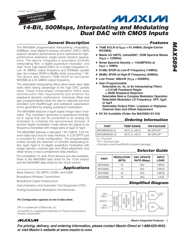
The MAX5894 is an advanced 14-bit, 500Msps Interpolating and Modulating Dual DAC designed for high-speed RF signal synthesis. Featuring programmable interpolation filters and a quadrature modulator, it provides superior dynamic performance optimized for broadband single-carrier transmit applications. This manual details the device’s technical specifications, selectable modulation modes (2x/4x/8x), and robust integration features. It is ideal for engineers developing complex telecommunication base stations targeting 3G UMTS, CDMA, GSM, or other high-performance wireless transmitters.
📄 Preview PAGE OF 32

Page 1 Text Content

19-3631; Rev 2; 10/08

EVALUATION KIT AVAILABLE

14-Bit, 500Msps, Interpolating and Modulating

Dual DAC with CMOS Inputs

General Description Features

INTERPOLATING FILTERS

The MAX5894 programmable interpolating, modulating, 74d B ACLR at f OUT = 61.44MHz (Single-Carrier 500Msps, dual digital-to-analog converter (DAC) offers WCDMA) ODULATOR superior dynamic performance and is optimized for high-

Meets 3G UMTS, cdma2000®, GSM Spectral Masks

performance wideband, single-carrier transmit applica-

(f OUT = 122MHz) INTERPOLATING

tions. The device integrates a selectable 2x/4x/8x FILTERS

Noise Spectral Density = -154d BFS/Hz at

interpolating filter, a digital quadrature modulator, and

f OUT = 16MHz

dual 14-bit, high-speed DACs on a single integrated cir-

DATA SYNCH

cuit. At 30MHz output frequency and 500Msps update 91d Bc SFDR at Low-IF Frequency (10MHz) AND DEM UX rate, the in-band SFDR is 86d Bc while consuming 1.1W.

88d Bc SFDR at High-IF Frequency (50MHz)

The device also delivers 73d B ACLR for two-carrier

Low Power: 886m W (f CLK = 250MHz)

WCDMA at a 61.44MHz output frequency.

User Programmable

The selectable interpolating filters allow lower input data

Selectable 2x, 4x, or 8x Interpolating Filters

rates while taking advantage of the high DAC update

< 0.01d B Passband Ripple

rates. These linear-phase interpolation filters ease

> 99d B Stopband Rejection

reconstruction filter requirements and enhance the

Selectable Real or Complex Modulator Operation

passband dynamic performance. Individual offset and

Selectable Modulator LO Frequency: OFF, f IM/2

gain programmability allow the user to calibrate out local

or f IM/4

oscillator (LO) feedthrough and sideband suppression

Selectable Output Filter: Lowpass or Highpass

errors generated by analog quadrature modulators.

Channel Gain and Offset Adjustment

The MAX5894 features a f IM/4 digital image-reject mod-

EV Kit Available (Order the MAX5894 EV Kit)

ulator. This modulator generates a quadrature-modulat- ed IF signal that can be presented to an analog I/Q

Ordering Information

modulator to complete the upconversion process. A second digital modulation mode allows the signal to be

PART TEMP RANGE PIN-PACKAGE

frequency-translated with image pairs at f IM/2 or f IM/4.

MAX5894EGK-D -40°C to +85°C 68 QFN-EP*

The MAX5894 features a standard 1.8V CMOS, 3.3V tol-

MAX5894EGK+D -40°C to +85°C 68 QFN-EP*

erant data input bus for easy interface. A 3.3V SPI™ port

is provided for mode configuration. The programmable D = Dry pack. modes include the selection of 2x/4x/8x interpolating fil- *EP = Exposed pad. +Denotes a lead-free/Ro HS-compliant package.

ters, f IM/2, f IM/4 or no digital quadrature modulation with image rejection, channel gain and offset adjustment, and

Selector Guide

offset binary or two’s complement data interface. Pin-compatible 12- and 16-bit devices are also available.

RESOLUTION DAC UPDATE INPUT

Refer to the MAX5893 data sheet for the 12-bit version PART

(BITS) RATE (Msps) LOGIC

and the MAX5895 data sheet for the 16-bit version.

MAX5893 CMOS

Applications

MAX5894 CMOS

Base Stations: 3G UMTS, CDMA, and GSM MAX5895 CMOS Broadband Wireless Transmitters MAX5898 LVDS Broadband Cable Infrastructure

Simplified Diagram

Instrumentation and Automatic Test Equipment (ATE) Analog Quadrature Modulation Architectures

DATA OUTI DAC

PORT A

Pin Configuration appears at end of data sheet.

DATACLK

SPI is a trademark of Motorola, Inc. DAC

PORT B

cdma2000 is a registered trademark of Telecommunications Industry Association.

Maxim Integrated Products

For pricing, delivery, and ordering information, please contact Maxim Direct at 1-888-629-4642, or visit Maxim’s website at www.maxim-ic.com.

Page Summary Contents For MAXIM MAX5894 14-Bit, 500 Msps, Interpolating and Modulating Dual DAC with CMOS Inputs

Page 1 19-3631; Rev 2; 10/08 EVALUATION KIT AVAILABLE 14-Bit, 500Msps, Interpolating and Modulating Dual DAC with CMOS Inputs General Description Features INTERPOLATING FILTERS The MAX5894 programmable inter...
Page 2 14-Bit, 500Msps, Interpolating and Modulating Dual DAC with CMOS Inputs ABSOLUTE MAXIMUM RATINGS DVDD1.8, AVDD1.8 to GND, DACREF ..................-0.3V to +2.16V DOUT, DATACLK, DATACLK/B12 Continuous...
Page 3 14-Bit, 500Msps, Interpolating and Modulating Dual DAC with CMOS Inputs ELECTRICAL CHARACTERISTICS (continued) (DVDD1.8 = AVDD1.8 = 1.8V, AVCLK = AVDD3.3 = DVDD3.3 = 3.3V, modulator off, 2x interpolat...
Page 4 14-Bit, 500Msps, Interpolating and Modulating Dual DAC with CMOS Inputs ELECTRICAL CHARACTERISTICS (continued) (DVDD1.8 = AVDD1.8 = 1.8V, AVCLK = AVDD3.3 = DVDD3.3 = 3.3V, modulator off, 2x interpolat...
Page 5 14-Bit, 500Msps, Interpolating and Modulating Dual DAC with CMOS Inputs ELECTRICAL CHARACTERISTICS (continued) (DVDD1.8 = AVDD1.8 = 1.8V, AVCLK = AVDD3.3 = DVDD3.3 = 3.3V, modulator off, 2x interpolat...
Page 6 14-Bit, 500Msps, Interpolating and Modulating Dual DAC with CMOS Inputs ELECTRICAL CHARACTERISTICS (continued) (DVDD1.8 = AVDD1.8 = 1.8V, AVCLK = AVDD3.3 = DVDD3.3 = 3.3V, modulator off, 2x interpolat...
Page 7 SF DR (d Bc SF DR (d Bc SF DR (d Bc 14-Bit, 500Msps, Interpolating and Modulating Dual DAC with CMOS Inputs Typical Operating Characteristics (DVDD1.8 = AVDD1.8 = 1.8V, AVCLK = AVDD3.3 = DVDD3.3 = 3.3...
Page 8 GA IN IS AT CH (d B) SU PP LY UR RE NT (m A) 14-Bit, 500Msps, Interpolating and Modulating Dual DAC with CMOS Inputs Typical Operating Characteristics (continued) (DVDD1.8 = AVDD1.8 = 1.8V, AVCLK = AV...
Page 9 OU TP UT OW ER (d Bm AC LR (d B) 14-Bit, 500Msps, Interpolating and Modulating AC LR d B Dual DAC with CMOS Inputs AC LR d B CA RR IE -1 4d Bm Typical Operating Characteristics (continued) (DVDD1.8 = ...
Page 10 14-Bit, 500Msps, Interpolating and Modulating Dual DAC with CMOS Inputs Pin Description PIN NAME FUNCTION CLKP Noninverting Differential Clock Input. Internally biased to AVCLK/2. CLKN Inverting Diffe...
Page 11 14-Bit, 500Msps, Interpolating and Modulating Dual DAC with CMOS Inputs Pin Description (continued) PIN NAME FUNCTION UX UX Low Analog Power Supply. Accepts a 1.71V to 1.89V supply range. Bypass each ...
Page 12 14-Bit, 500Msps, Interpolating and Modulating Dual DAC with CMOS Inputs Detailed Description The power-down modes can be used to turn off each DAC’s output current or the entire digital section. The M...
Page 13 14-Bit, 500Msps, Interpolating and Modulating Dual DAC with CMOS Inputs When writing to the MAX5894, data is shifted into DIN; read operation. The most significant bit (MSB) is shifted data is shifted...
Page 14 14-Bit, 500Msps, Interpolating and Modulating Dual DAC with CMOS Inputs t SDS t SDH t SDV Figure 3. SPI Serial-Interface Timing Diagram
Page 15 14-Bit, 500Msps, Interpolating and Modulating Dual DAC with CMOS Inputs Programming Registers of the registers. The following are descriptions of each Programming its registers with the SPI serial int...
Page 16 14-Bit, 500Msps, Interpolating and Modulating Dual DAC with CMOS Inputs Address 00h e-jw (default), cancelling the upper image when used with an external quadrature mod- Bit 6 Logic 0 (default) causes...
Page 17 14-Bit, 500Msps, Interpolating and Modulating Dual DAC with CMOS Inputs Address 07h and 08h for the I- and Q-channel, respectively. The range of coarse is from 0 to 15, with 15 being the Bit 7 Logic 0...
Page 18 14-Bit, 500Msps, Interpolating and Modulating Dual DAC with CMOS Inputs tionship and detects if the phase drifts more than ±1 Table 4. Clock Frequency Ratios in data clock cycle. If this occurs, the s...
Page 19 14-Bit, 500Msps, Interpolating and Modulating GA IN (d BF S) GA IN (d BF S) Dual DAC with CMOS Inputs Interpolating Filter ter is located after the modulator. In the 8x interpolation The MAX5894 featu...
Page 20 14-Bit, 500Msps, Interpolating and Modulating Dual DAC with CMOS Inputs The programmable interpolation filters multiply the 2) Lower input data rates eliminate board-level high- MAX5894 input data rat...
Page 21 14-Bit, 500Msps, Interpolating and Modulating Dual DAC with CMOS Inputs images at odd numbers of f S are filtered. At the output of 10f S, etc. Finally, the third filter removes images at 4f S, the fi...
Page 22 14-Bit, 500Msps, Interpolating and Modulating Dual DAC with CMOS Inputs FILTER RESPONSE NO INTERPOLATIONSIGNAL IMAGE INPUT SPECTRUM AND FIRST FILTER RESPONSE SIGNAL IMAGE 2x INTERPOLATION OUTPUT SPECT...
Page 23 14-Bit, 500Msps, Interpolating and Modulating Dual DAC with CMOS Inputs FILTER RESPONSE NO INTERPOLATIONSIGNAL IMAGE INPUT SPECTRUM AND FIRST FILTER RESPONSE SIGNAL IMAGE 2x INTERPOLATION OUTPUT SPECT...
Page 24 14-Bit, 500Msps, Interpolating and Modulating Dual DAC with CMOS Inputs Digital Modulator The outputs of the modulator can be expressed as: The MAX5894 features digital modulation at frequencies of f ...
Page 25 14-Bit, 500Msps, Interpolating and Modulating Dual DAC with CMOS Inputs Power-Down Mode Data Clock The MAX5894 features three power-saving modes. The MAX5894 features synchronizers that allow for arbi...
Page 26 14-Bit, 500Msps, Interpolating and Modulating Dual DAC with CMOS Inputs sources directly to the device without external resistors clock source, however it is recommended to use to define the DC level....
Page 27 14-Bit, 500Msps, Interpolating and Modulating Dual DAC with CMOS Inputs If a transformer is not used, the outputs must have a resistive termination to ground. Figure 17 shows the MAX5894 output config...
Page 28 14-Bit, 500Msps, Interpolating and Modulating Dual DAC with CMOS Inputs REFIO must be buffered with an external amplifier, if heavy rent IOUT for the differential current outputs of the DAC. loading i...
Page 29 14-Bit, 500Msps, Interpolating and Modulating Dual DAC with CMOS Inputs Power Supplies, Bypassing, Static Performance Parameter Decoupling, and Layout Definitions Grounding and power-supply decoupling...
Page 30 14-Bit, 500Msps, Interpolating and Modulating Dual DAC with CMOS Inputs However, noise sources such as thermal noise, refer- Two-/Four-Tone Intermodulation ence noise, clock jitter, etc., affect the i...
Page 31 14-Bit, 500Msps, Interpolating and Modulating Dual DAC with CMOS Inputs Pin Configuration TOP VIEW A4 AV CL A3 AV DD 1. DV DD 1. 8A2 AV DD 3. CLKP EXPOSED PAD DACREF CLKN REFIO A0A1 OU TI N.C. RESET N...
Page 32 14-Bit, 500Msps, Interpolating and Modulating Dual DAC with CMOS Inputs Revision History REVISION REVISION PAGES DESCRIPTION NUMBER DATE CHANGED Initial release 4/07 10/08 Add note to setup and hold s...

Manual Details

Brand Dual
Pages 32
File Size 294.96 KB
Published May 30, 2026
69 views

Enter the captcha to get the download link:

captcha

Frequently Asked Questions

What is the primary functionality of the MAX5894 module?

It is an interpolating and modulating dual DAC that generates a quadrature-modulated IF signal.

Can I change the interpolation rate of the device?

Yes, it features selectable 2x, 4x, or 8x interpolating filters rates.

What interface must be used for mode configuration?

A 3.3V SPI™ port is provided for mode configuration.

What are the operating temperature specifications?

The device's operating temperature range is -40°C to +85°C.