MAXIM MAX5893 12-Bit, 500Msps Interpolating and Modulating Dual DAC with CMOS Inputs
Summary
The MAX5893 is a professional-grade 12-Bit, 500Msps Interpolating and Modulating Dual DAC designed for advanced broadband wireless transmitters and base station infrastructure. It offers superior dynamic performance essential for wideband single-carrier applications, supporting standards like WCDMA, UMTS, and GSM. This manual provides complete documentation on the device's core capabilities, detailing its user-programmable features such as selectable interpolating filters, digital quadrature modulation, channel gain adjustment, and precise integration specifications for electrical engineers and RF designers.
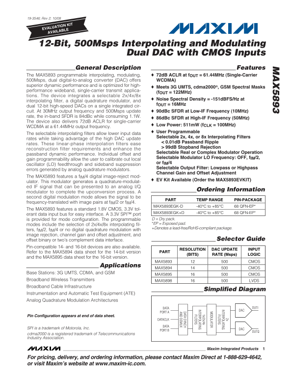
Page 1 Text Content
19-3546; Rev 2; 10/08
EVALUATION KIT AVAILABLE
12-Bit, 500Msps Interpolating and Modulating
Dual DAC with CMOS Inputs
General Description Features INTERPOLATING
FILTERS
The MAX5893 programmable interpolating, modulating, 72d B ACLR at f OUT = 61.44MHz (Single-Carrier 500Msps, dual digital-to-analog converter (DAC) offers WCDMA) ODULATOR superior dynamic performance and is optimized for high-
Meets 3G UMTS, cdma2000®, GSM Spectral Masks 1x/2x/4x
performance wideband, single-carrier transmit applica-
(f OUT = 122MHz) INTERPOLATING
tions. The device integrates a selectable 2x/4x/8x FILTERS
Noise Spectral Density = -151d BFS/Hz at
interpolating filter, a digital quadrature modulator, and
f OUT = 16MHz
dual 12-bit high-speed DACs on a single integrated cir- DATA SYNCH
cuit. At 30MHz output frequency and 500Msps update 90d Bc SFDR at Low-IF Frequency (10MHz) AND DEM UX
rate, the in-band SFDR is 84d Bc while consuming 1.1W.
86d Bc SFDR at High-IF Frequency (50MHz)
The device also delivers 72d B ACLR for single-carrier
Low Power: 511m W (f CLK = 100MHz)
WCDMA at a 61.44MHz output frequency.
User Programmable
The selectable interpolating filters allow lower input data
Selectable 2x, 4x, or 8x Interpolating Filters
rates while taking advantage of the high DAC update
< 0.01d B Passband Ripple
rates. These linear-phase interpolation filters ease
> 99d B Stopband Rejection
reconstruction filter requirements and enhance the
Selectable Real or Complex Modulator Operation
passband dynamic performance. Individual offset and
Selectable Modulator LO Frequency: OFF, f IM/2,
gain programmability allow the user to calibrate out local
or f IM/4
oscillator (LO) feedthrough and sideband suppression
Selectable Output Filter: Lowpass or Highpass
errors generated by analog quadrature modulators.
Channel Gain and Offset Adjustment
The MAX5893 features a f IM/4 digital image-reject mod-
EV Kit Available (Order the MAX5893EVKIT)
ulator. This modulator generates a quadrature-modulat- ed IF signal that can be presented to an analog I/Q
Ordering Information
modulator to complete the upconversion process. A second digital modulation mode allows the signal to be
PART TEMP RANGE PIN-PACKAGE
frequency-translated with image pairs at f IM/2 or f IM/4.
MAX5893EGK-D -40°C to +85°C 68 QFN-EP*
The MAX5893 features a standard 1.8V CMOS, 3.3V tol-
MAX5893EGK+D -40°C to +85°C 68 QFN-EP*
erant data input bus for easy interface. A 3.3V SPI™ port
is provided for mode configuration. The programmable D = Dry pack. *EP = Exposed pad.
modes include the selection of 2x/4x/8x interpolating fil-
+Denotes a lead-free/Ro HS-compliant package.
ters, f IM/2, f IM/4 or no digital quadrature modulation with image rejection, channel gain and offset adjustment, and
offset binary or two’s complement data interface. Selector Guide
Pin-compatible 14- and 16-bit devices are also available.
RESOLUTION DAC UPDATE INPUT
Refer to the MAX5894 data sheet for the 14-bit version PART
(BITS) RATE (Msps) LOGIC
and the MAX5895 data sheet for the 16-bit version.
MAX5893 CMOS
Applications
MAX5894 CMOS
Base Stations: 3G UMTS, CDMA, and GSM
MAX5895 CMOS
Broadband Wireless Transmitters MAX5898 LVDS Broadband Cable Infrastructure
Simplified Diagram
Instrumentation and Automatic Test Equipment (ATE) Analog Quadrature Modulation Architectures
DATA OUTI DAC
PORT A
Pin Configuration appears at end of data sheet.
DATACLK
SPI is a trademark of Motorola, Inc. DAC
PORT B
cdma2000 is a registered trademark of Telecommunications Industry Association.
Maxim Integrated Products
For pricing, delivery, and ordering information, please contact Maxim Direct at 1-888-629-4642, or visit Maxim’s website at www.maxim-ic.com.
Page Summary Contents For MAXIM MAX5893 12-Bit, 500Msps Interpolating and Modulating Dual DAC with CMOS Inputs
Manual Details
| Brand | Dual |
|---|---|
| Pages | 32 |
| File Size | 285.26 KB |
| Published | May 31, 2026 |
Enter the captcha to get the download link:

Frequently Asked Questions
What is the operational output frequency and update rate?
It features dual 12-bit high-speed DACs operating at 500Msps.
How does the device achieve excellent dynamic performance for communications standards?
It offers superior performance meeting 3G UMTS, cdma2000, and GSM Spectral Masks.
Can the hardware be configured to adjust signal properties?
Yes, it allows user programmability through channel gain/offset adjustment and selecting output filters (Lowpass or Highpass).
What is the required power consumption when operating at a 61.44MHz frequency for WCDMA?
The minimum power consumption is 511mW.