AD9216 10-Bit, 65/80/105 MSPS Dual Analog to Digital Converter Data Handbook Manual
Summary
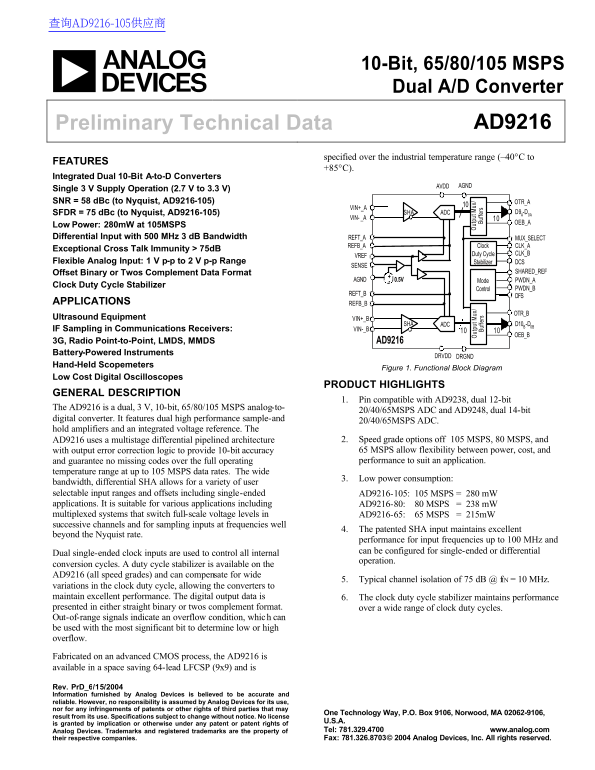
The AD9216 is a dual, high-performance 10-bit Analog-to-Digital Converter, available at speeds up to 105 MSPS. This manual offers comprehensive technical details on its differential pipelined architecture, low power consumption, and superior signal fidelity through features like clock duty cycle stabilization. It is designed for demanding field applications, making it ideal for communication receivers (3G/Radio), advanced ultrasound equipment, battery-powered instruments, oscilloscopes, and data acquisition systems requiring high accuracy and robust performance.
Page 1 Text Content
查询AD9216-105供应商
10-Bit, 65/80/105 MSPS Dual A/D Converter
Preliminary Technical Data AD9216
specified over the industrial temperature range (–40°C to
FEATURES
Integrated Dual 10-Bit A-to-D Converters
AVDD AGND
Single 3 V Supply Operation (2.7 V to 3.3 V) SNR = 58 d Bc (to Nyquist, AD9216-105) OTR_A
VIN+_A
SFDR = 75 d Bc (to Nyquist, AD9216-105) SHA ADC D9A-D0A
VIN- _A
OEB_A
Low Power: 280m W at 105MSPS Differential Input with 500 MHz 3 d B Bandwidth REFT_A MUX_SELECT
REFB_A Clock CLK_A
Exceptional Cross Talk Immunity > 75d B
Duty Cycle CLK_B
Flexible Analog Input: 1 V p-p to 2 V p-p Range Stabilizer DCSSENSE
Offset Binary or Twos Complement Data Format SHARED_REF
AGND 0.5V Mode PWDN_A
Clock Duty Cycle Stabilizer
Control PWDN_B
REFT_B
APPLICATIONS REFB_B
OTR_B
Ultrasound Equipment VIN+_B
SHA ADC D10B-D0B10
IF Sampling in Communications Receivers: VIN-_B
OEB_B
3G, Radio Point-to-Point, LMDS, MMDS AD9216 Battery-Powered Instruments
DRVDD DRGND
Hand-Held Scopemeters
Figure 1. Functional Block Diagram
Low Cost Digital Oscilloscopes
PRODUCT HIGHLIGHTS
GENERAL DESCRIPTION
1. Pin compatible with AD9238, dual 12-bit
The AD9216 is a dual, 3 V, 10-bit, 65/80/105 MSPS analog-to-
20/40/65MSPS ADC and AD9248, dual 14-bit
digital converter. It features dual high performance sample-and
20/40/65MSPS ADC.
hold amplifiers and an integrated voltage reference. The
AD9216 uses a multistage differential pipelined architecture 2. Speed grade options off 105 MSPS, 80 MSPS, and with output error correction logic to provide 10-bit accuracy 65 MSPS allow flexibility between power, cost, and and guarantee no missing codes over the full operating performance to suit an application.
temperature range at up to 105 MSPS data rates. The wide Ou tp ut ux
Ou tp ut ux
3. Low power consumption: Bu ffe rs
bandwidth, differential SHA allows for a variety of user Bu ffe rs
selectable input ranges and offsets including single-ended AD9216-105: 105 MSPS = 280 m W applications. It is suitable for various applications including AD9216-80: 80 MSPS = 238 m W multiplexed systems that switch full-scale voltage levels in AD9216-65: 65 MSPS = 215m W successive channels and for sampling inputs at frequencies well
4. The patented SHA input maintains excellent
beyond the Nyquist rate.
performance for input frequencies up to 100 MHz and can be configured for single-ended or differential
Dual single-ended clock inputs are used to control all internal
operation.
conversion cycles. A duty cycle stabilizer is available on the AD9216 (all speed grades) and can compensate for wide
5. Typical channel isolation of 75 d B @ f IN = 10 MHz.
variations in the clock duty cycle, allowing the converters to maintain excellent performance. The digital output data is 6. The clock duty cycle stabilizer maintains performance presented in either straight binary or twos complement format. over a wide range of clock duty cycles. Out-of-range signals indicate an overflow condition, which can be used with the most significant bit to determine low or high overflow.
Fabricated on an advanced CMOS process, the AD9216 is available in a space saving 64-lead LFCSP (9x9) and is
Rev. Pr D_6/15/2004 Information furnished by Analog Devices is believed to be accurate and reliable. However, no responsibility is assumed by Analog Devices for its use, nor for any infringements of patents or other rights of third parties that may
One Technology Way, P.O. Box 9106, Norwood, MA 02062-9106,
result from its use. Specifications subject to change without notice. No license
is granted by implication or otherwise under any patent or patent rights of
Analog Devices. Trademarks and registered trademarks are the property of Tel: 781.329.4700 www.analog.com
their respective companies. Fax: 781.326.8703 © 2004 Analog Devices, Inc. All rights reserved.
Page Summary Contents For AD9216 10-Bit, 65/80/105 MSPS Dual Analog to Digital Converter Data Handbook Manual
Manual Details
| Brand | Dual |
|---|---|
| Pages | 20 |
| File Size | 262.35 KB |
| Published | June 03, 2026 |
Enter the captcha to get the download link:

Frequently Asked Questions
What input frequencies can the ADC handle?
The patented SHA input maintains excellent performance for input frequencies up to 100 MHz.
How do I use an external reference voltage?
Tying the SENSE pin to AVDD will disable the internal reference, allowing you to select and implement an external reference source.
What is the AD9216's clock stability feature?
It features a duty cycle stabilizer that maintains excellent performance over a wide range of clock duty cycles.