Vishay K814P K824P K844P User Guide and Specifications
Summary
These Vishay optocouplers (K814P series) utilize phototransistor technology to provide robust electrical isolation, featuring single, dual, and quad channels suitable for demanding communication systems. Designed for applications like PBX, fax machines, and feature phones, they boast high isolation voltages up to 5000V and low capacitance. This manual provides comprehensive technical data, including detailed switching characteristics, operating parameters, and isolation testing guidelines essential for reliable component integration.
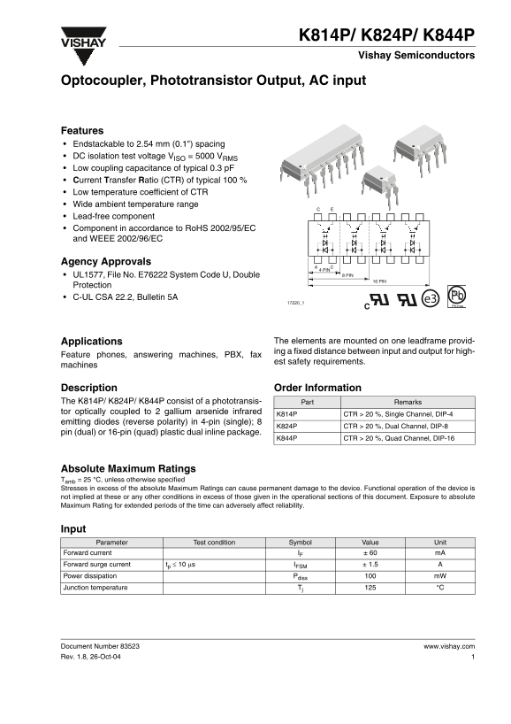
Page 1 Text Content
K814P/ K824P/ K844P Vishay Semiconductors
Optocoupler, Phototransistor Output, AC input
Features Endstackable to 2.54 mm (0.1") spacing DC isolation test voltage VISO = 5000 VRMS Low coupling capacitance of typical 0.3 p F Current Transfer Ratio (CTR) of typical 100 % Low temperature coefficient of CTR Wide ambient temperature range Lead-free component Component in accordance to Ro HS 2002/95/EC and WEEE 2002/96/EC
Agency Approvals
UL1577, File No. E76222 System Code U, Double PIN
Protection
C-UL CSA 22.2, Bulletin 5A e3 Pb
Pb-free
Applications The elements are mounted on one leadframe provid- ing a fixed distance between input and output for high-
Feature phones, answering machines, PBX, fax
est safety requirements.
machines
Description Order Information The K814P/ K824P/ K844P consist of a phototransis- Part Remarks tor optically coupled to 2 gallium arsenide infrared
K814P CTR > 20 %, Single Channel, DIP-4
emitting diodes (reverse polarity) in 4-pin (single); 8
K824P CTR > 20 %, Dual Channel, DIP-8
pin (dual) or 16-pin (quad) plastic dual inline package.
K844P CTR > 20 %, Quad Channel, DIP-16
Absolute Maximum Ratings Tamb = 25 °C, unless otherwise specified Stresses in excess of the absolute Maximum Ratings can cause permanent damage to the device. Functional operation of the device is not implied at these or any other conditions in excess of those given in the operational sections of this document. Exposure to absolute Maximum Rating for extended periods of the time can adversely affect reliability.
Input Parameter Test condition Symbol Value Unit
Forward current IF ± 60 m A
Forward surge current tp ≤ 10 µs IFSM ± 1.5 Power dissipation Pdiss m W Junction temperature Tj °C
Document Number 83523 www.vishay.com Rev. 1.8, 26-Oct-04
Page Summary Contents For Vishay K814P K824P K844P User Guide and Specifications
Manual Details
| Brand | Vishay |
|---|---|
| Pages | 9 |
| File Size | 257.89 KB |
| Published | June 01, 2026 |
Enter the captcha to get the download link:

Frequently Asked Questions
What certifications confirm the device's compliance and safety features?
The components are compliant with RoHS and WEEE standards, and also feature UL1577 certification.
What is the maximum isolation voltage provided by the optocouplers?
It offers an AC Isolation test voltage (RMS) of 5000 V.
What is the typical ambient temperature operating range for this device?
The device operates in a wide ambient temperature range from -40 °C to +100 °C.
Are these semiconductors suitable for medical applications?
No; they are not designed for use in medical, life-saving, or life-sustaining applications.