Vishay ILD615 ILQ615 Data Handbook
Summary
The ILD615 and ILQ615 are high-performance optocouplers designed for industrial data I/O and control systems. These dual or quad channel devices utilize phototransistor outputs with GaAs IRLED emitters, offering superior isolation voltage and enhanced electrical noise immunity in challenging environments. This technical manual provides comprehensive documentation for engineers, detailing operating parameters, compliance standards (UL/CSA), and application guidelines necessary for implementing reliable medium-speed signal transfer solutions into your design.
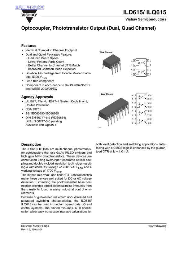
Page 1 Text Content
查询ILD615供应商
ILD615/ ILQ615
VISHAY
Vishay Semiconductors
Optocoupler, Phototransistor Output (Dual, Quad Channel)
Features Identical Channel to Channel Footprint
Dual Channel
Dual and Quad Packages Feature: - Reduced Board Space - Lower Pin and Parts Count - Better Channel to Channel CTR Match - Improved Common Mode Rejection Isolation Test Voltage from Double Molded Pack- age, 5300 VRMS Lead-free component Component in accordance to Ro HS 2002/95/EC and WEEE 2002/96/EC
Quad Channel
Agency Approvals UL1577, File No. E52744 System Code H or J, Double Protection CSA 93751 BSI IEC60950 IEC60965 DIN EN 60747-5-2 (VDE0884) DIN EN 60747-5-5 pending Available with Option 1
Description both level detection and switching applications. Inter- facing with a CMOS logic is enhanced by the guaran-
The ILD615/ ILQ615 are multi-channel phototransis-
teed CTR at IF = 1.0 m A.
tor optocouplers that use Ga As IRLED emitters and high gain NPN phototransistors. These devices are constructed using over/under leadframe optical cou- pling and double molded insulation technology result- ing a withstand test voltage of 7500 VACPEAK and a working voltage of 1700 VRMS. The binned min./max. and linear CTR characteristics make these devices well suited for DC or AC voltage detection. Eliminating the phototransistor base con- nection provides added electrical noise immunity from the transients found in many industrial control envi- ronments. Because of guaranteed maximum non-saturated and saturated switching characteristics, the ILD615/ ILQ615 can be used in medium speed data I/O and control systems. The binned min./max. CTR specifi- cation allow easy worst case interface calculations for
Document Number 83652 www.vishay.com Rev. 1.3, 19-Apr-04
Page Summary Contents For Vishay ILD615 ILQ615 Data Handbook
Manual Details
| Brand | Vishay |
|---|---|
| Pages | 11 |
| File Size | 159.85 KB |
| Published | June 05, 2026 |
Enter the captcha to get the download link:

Frequently Asked Questions
What are the materials certifications for these optocouplers?
The components are lead-free and comply with RoHS (2002/95/EC) and WEEE (2002/96/EC).
What is the maximum isolation test voltage?
The stated isolation test voltage is 5300 V RMS at I = 1.0 sec.
How does it perform in electrical noise environments?
By eliminating the phototransistor base connection, the device provides added electrical noise immunity from industrial control transients.
What types of applications are these devices suited for?
They can be used in medium-speed data I/O and control systems due to guaranteed switching characteristics.