Vishay BF988 Data Handbook
Summary
This document provides comprehensive technical specifications for the BF988 N-Channel Dual Gate MOS-FET, a high-performance, depletion mode component optimized for sensitive radio frequency applications. Ideal for engineers designing input/mixer stages and VHF/UHF tuners requiring low noise figures, high gain, and stable operation across varying AGC ranges. The manual details electrical characteristics, s-parameters (AC/DC), power ratings, and recommended handling procedures, enabling precise integration into complex RF circuitry.
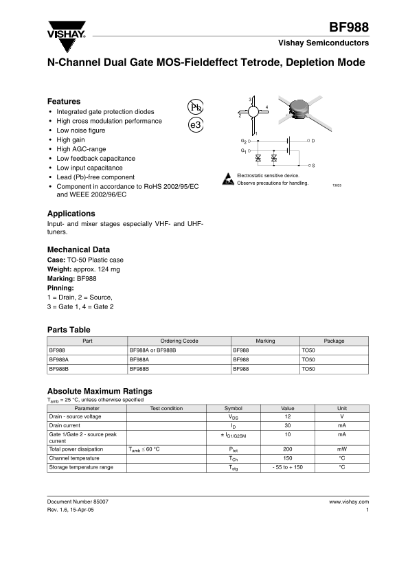
Page 1 Text Content
BF988
Vishay Semiconductors
N-Channel Dual Gate MOS-Fieldeffect Tetrode, Depletion Mode
Features Integrated gate protection diodes High cross modulation performance
Low noise figure High gain G2 High AGC-range G1 Low feedback capacitance Low input capacitance
Electrostatic sensitive device.
Lead (Pb)-free component
Observe precautions for handling.
Component in accordance to Ro HS 2002/95/EC and WEEE 2002/96/EC
Applications Input- and mixer stages especially VHF- and UHF- tuners.
Mechanical Data Case: TO-50 Plastic case Weight: approx. 124 mg Marking: BF988 Pinning: 1 = Drain, 2 = Source, 3 = Gate 1, 4 = Gate 2
Parts Table
Part Ordering Ccode Marking Package
BF988 BF988A or BF988B BF988 TO50
BF988A BF988A BF988 TO50 BF988B BF988B BF988 TO50
Absolute Maximum Ratings Tamb = 25 °C, unless otherwise specified
Parameter Test condition Symbol Value Unit
Drain - source voltage VDS Drain current ID m A Gate 1/Gate 2 - source peak ± IG1/G2SM m A current
Total power dissipation Tamb ≤ 60 °C Ptot m W
Channel temperature TCh °C Storage temperature range Tstg - 55 to + 150 °C
Document Number 85007 www.vishay.com Rev. 1.6, 15-Apr-05
Page Summary Contents For Vishay BF988 Data Handbook
Manual Details
| Brand | Vishay |
|---|---|
| Pages | 9 |
| File Size | 158.57 KB |
| Published | May 31, 2026 |
Enter the captcha to get the download link:

Frequently Asked Questions
What are the recommended limits for power dissipation?
The maximum total power dissipation is 200 mW when the ambient temperature is less than or equal to 60°C.
How should I handle this device based on its sensitivity?
It is an electrostatic sensitive device, so users must observe precautions for proper handling.
What are the pin functions (drain, source, gate)?
Pin 1 is Drain, Pin 2 is Source, Pin 3 is Gate 1, and Pin 4 is Gate 2.
Is this component compliant with major environmental directives?
Yes, it is a Lead (Pb)-free component and complies with RoHS and WEEE directives.