Vishay IL211AT 212AT 213AT Specifications and User Guide
Summary
Maintain high electrical isolation in your designs with this advanced optocoupler series. Featuring a Gallium Arsenide LED and phototransistor output in a surface-mount SOIC-8 package, these components provide reliable signal transfer while offering up to 3000 V RMS isolation voltage. This manual provides detailed technical specifications on Current Transfer Ratio (CTR), switching times, and absolute maximum ratings. Ideal for engineers building compact, high-density electronics systems requiring robust electrical separation between input and output circuits.
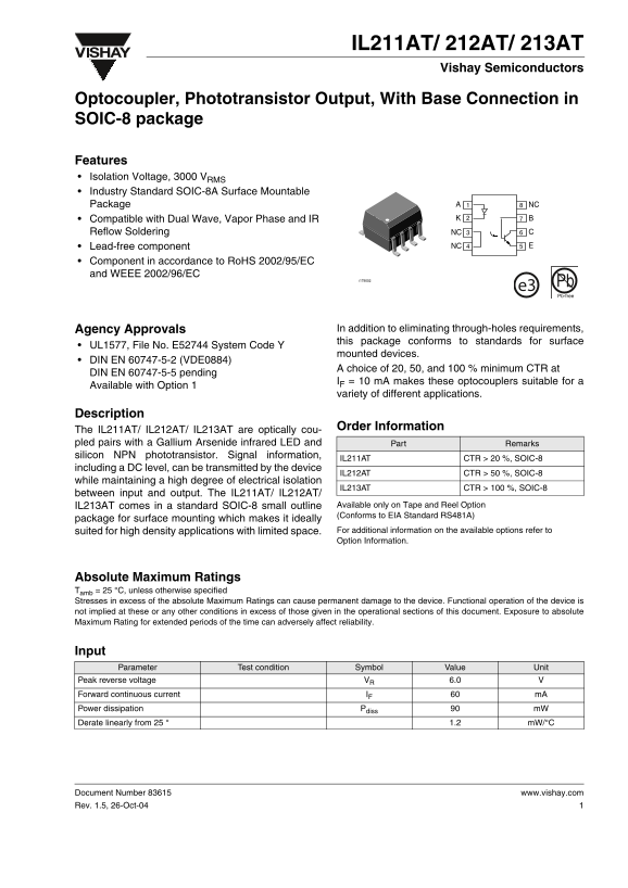
Page 1 Text Content
IL211AT/ 212AT/ 213AT
Vishay Semiconductors
Optocoupler, Phototransistor Output, With Base Connection in SOIC-8 package
Features Isolation Voltage, 3000 VRMS Industry Standard SOIC-8A Surface Mountable
Package NC
Compatible with Dual Wave, Vapor Phase and IR
Reflow Soldering NC Lead-free component NC
Component in accordance to Ro HS 2002/95/EC and WEEE 2002/96/EC
e3 Pb Pb-free
Agency Approvals In addition to eliminating through-holes requirements, this package conforms to standards for surface
UL1577, File No. E52744 System Code Y
mounted devices.
DIN EN 60747-5-2 (VDE0884)
A choice of 20, 50, and 100 % minimum CTR at
DIN EN 60747-5-5 pending
IF = 10 m A makes these optocouplers suitable for a
Available with Option 1
variety of different applications.
Description
Order Information
The IL211AT/ IL212AT/ IL213AT are optically cou- pled pairs with a Gallium Arsenide infrared LED and Part Remarks silicon NPN phototransistor. Signal information,
IL211AT CTR > 20 %, SOIC-8
including a DC level, can be transmitted by the device
IL212AT CTR > 50 %, SOIC-8
while maintaining a high degree of electrical isolation
IL213AT CTR > 100 %, SOIC-8
between input and output. The IL211AT/ IL212AT/
IL213AT comes in a standard SOIC-8 small outline Available only on Tape and Reel Option (Conforms to EIA Standard RS481A)
package for surface mounting which makes it ideally
suited for high density applications with limited space. For additional information on the available options refer to Option Information.
Absolute Maximum Ratings Tamb = 25 °C, unless otherwise specified Stresses in excess of the absolute Maximum Ratings can cause permanent damage to the device. Functional operation of the device is not implied at these or any other conditions in excess of those given in the operational sections of this document. Exposure to absolute Maximum Rating for extended periods of the time can adversely affect reliability.
Input Parameter Test condition Symbol Value Unit
Peak reverse voltage VR 6.0
Forward continuous current IF m A Power dissipation Pdiss m W Derate linearly from 25 1.2 m W/°C
Document Number 83615 www.vishay.com Rev. 1.5, 26-Oct-04
Page Summary Contents For Vishay IL211AT 212AT 213AT Specifications and User Guide
Manual Details
| Brand | Vishay |
|---|---|
| Pages | 7 |
| File Size | 156.96 KB |
| Published | June 05, 2026 |
Enter the captcha to get the download link:
