Vishay AN606 Data Sheet
Summary
Vishay Siliconix Current-Sensing Power MOSFETs offer an efficient solution for implementing robust overcurrent and short-circuit protection in high-power circuits. This manual provides comprehensive technical details on integrating the embedded current-sensing feature, covering optimized package designs (DPAK), circuit principles using op-amps/comparators, and practical design guidelines. Ideal for electrical engineers and designers working on supervisory protective functions, these devices ensure reliable system safety with minimal external components.
Page 1 Text Content
AN606 Vishay Siliconix
Current-Sensing Power MOSFETs
Kandarp Pandya
INTRODUCTION
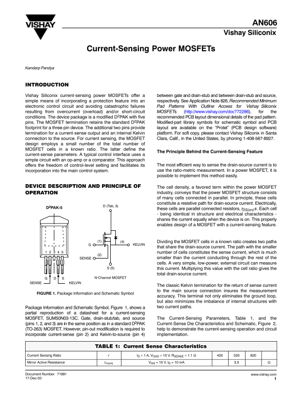
Vishay Siliconix current-sensing power MOSFETs offer a between gate and drain-stub and between drain-stub and source, simple means of incorporating a protection feature into an respectively. See Application Note 826, Recommended Minimum electronic control circuit and avoiding catastrophic failures Pad Patterns With Outline Access for Vishay Siliconix resulting from overcurrent (overload) and/or short-circuit MOSFETs (http://www.vishay.com/doc?72286), for the conditions. The device package is a modified D2PAK with five recommended PCB layout dimensional details of the pad pattern. pins. The MOSFET termination retains the standard D2PAK Modified-part library symbols for schematic symbol and PCB footprint for a three-pin device. The additional two pins provide layout are available on the “Protel” (PCB design software) termination for a current-sense output and an internal Kelvin platform. For soft copy, please contact Vishay Siliconix in Santa connection to the source. For current sensing, the MOSFET Clara, Calif., in the United States, by phoning 1-408-567-8927.
design employs a small number of the total number of MOSFET cells in a known ratio. The latter define the
The Principle Behind the Current-Sensing Feature
current-sense parameters. A typical control interface uses a simple circuit with an op-amp or a comparator. This approach
offers the freedom of control-level setting and facilitates its The most efficient way to sense the drain-source current is to incorporation into the main control system. use the ratio-metric measurement. In a power MOSFET, it is possible to implement this method easily.
DEVICE DESCRIPTION AND PRINCIPLE OF The cell density, a favored term within the power MOSFET
OPERATION industry, conveys that the power MOSFET structure consists of many cells connected in parallel. In principle, these cells constitute a resistive path for drain-source current. Electrically,
D (Tab, 3)
D2PAK-5 these cells are parallel connected resistors, r DS(on)s. Each cell
- being identical in structure and electrical characteristics - shares the current equally when the device is on. This property enables design of a MOSFET with a current-sensing feature.
(1) (4) Dividing the MOSFET cells in a known ratio creates two paths
KELVIN
that share the drain-source current. The path with the smaller number of cells constitutes the sense current, which is much
SENSE smaller than the current conducting through the rest of the cells. A very simple, low-power, external circuit can measure
S (5) this current. Multiplying this value with the cell ratio gives the
total drain-source current.
SG N-Channel MOSFET
SENSE KELVIN
The classic Kelvin termination for the return of sense current to the main source connection insures the measurement
FIGURE 1. Package Information and Schematic Symbol
accuracy. This terminal not only eliminates the ground loop, but also minimizes the imbalance of internal structures with Package Information and Schematic Symbol, Figure 1, shows a two current paths.
partial reproduction of a datasheet for a current-sensing
MOSFET, SUM50N03-13C. Gate, drain-stub/tab, and source The Current-Sensing Parameters, Table 1, and the (pins 1, 2, and 3) are in the same position as in a standard D2PAK Current-Sense Die Characteristics and Schematic, Figure 2, (TO-263) MOSFET. However, pin-out modification is required to help to demonstrate the current-sensing operation and circuit incorporate current-sense (pin 2) and Kelvin-to-source (pin 4) implementation.
TABLE 1: Current Sense Characteristics
Current Sensing Ratio ID = 1 A, VGSS = 10 V, RSENSE = 1.1 Mirror Active Resistance rm(on) VGS = 10 V, ID = 10 m A 3.5
Document Number: 71991 www.vishay.com 17-Dec-03
Page Summary Contents For Vishay AN606 Data Sheet
Manual Details
| Brand | Vishay |
|---|---|
| Pages | 4 |
| File Size | 68.93 KB |
| Published | June 05, 2026 |
Enter the captcha to get the download link:

Frequently Asked Questions
What primary protection benefits do these MOSFETs provide?
They enable the incorporation of supervisory features like overcurrent and/or short-circuit protection.
How does the current-sensing feature operate internally?
It divides the MOSFET cells into a known ratio, creating two paths that share the drain-source current. One path serves as the sense signal.
Is this device suitable for precise current control applications?
No, while flexible for circuit design, its measurement accuracy is not recommended for dedicated current-control applications.
What physical design modifications are required for current sensing?
The device requires significant pin-out modification to incorporate separate pins for the sense current and Kelvin connection to the source.