Vishay 6N1135 6N1136 Data Sheet
Summary
This comprehensive guide provides detailed specifications for 6N1135 and (or) 6N1136 high-speed optocouplers from Vishay Semiconductors. Designed for industrial electronics, these components offer safe signal transmission between isolated circuits up to 2.0 MHz. The manual details absolute maximum ratings, input/output parameters, switching characteristics, and technical options, making it essential reading for electrical engineers and hardware designers who require reliable, isolated coupling solutions for their complex circuit designs.
Page 1 Text Content
6N1135/ 6N1136 Vishay Semiconductors
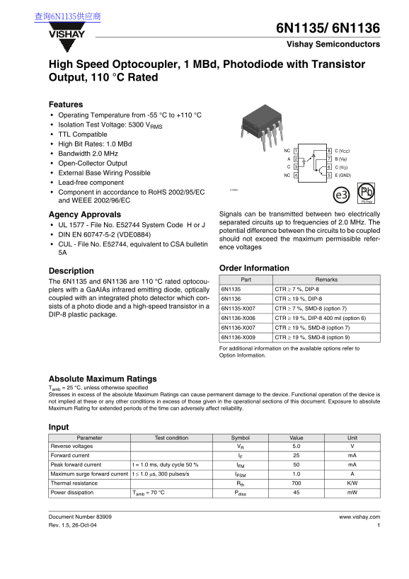
High Speed Optocoupler, 1 MBd, Photodiode with Transistor Output, 110 °C Rated
Features Operating Temperature from -55 °C to +110 °C Isolation Test Voltage: 5300 VRMS TTL Compatible High Bit Rates: 1.0 MBd
(VCC)NC
Bandwidth 2.0 MHz
Open-Collector Output
External Base Wiring Possible
NC (GND)
Lead-free component
Component in accordance to Ro HS 2002/95/EC Pb
and WEEE 2002/96/EC Pb-free
Agency Approvals Signals can be transmitted between two electrically separated circuits up to frequencies of 2.0 MHz. The
UL 1577 - File No. E52744 System Code H or J
potential difference between the circuits to be coupled
DIN EN 60747-5-2 (VDE0884)
should not exceed the maximum permissible refer-
CUL - File No. E52744, equivalent to CSA bulletin
ence voltages
Order Information
Description
Part Remarks
The 6N1135 and 6N1136 are 110 °C rated optocou-
plers with a Ga AIAs infrared emitting diode, optically 6N1135 CTR ≥ 7 %, DIP-8
coupled with an integrated photo detector which con- 6N1136 CTR ≥ 19 %, DIP-8 sists of a photo diode and a high-speed transistor in a
6N1135-X007 CTR ≥ 7 %, SMD-8 (option 7)
DIP-8 plastic package.
6N1136-X006 CTR ≥ 19 %, DIP-8 400 mil (option 6) 6N1136-X007 CTR ≥ 19 %, SMD-8 (option 7)
6N1136-X009 CTR ≥ 19 %, SMD-8 (option 9)
For additional information on the available options refer to Option Information.
Absolute Maximum Ratings Tamb = 25 °C, unless otherwise specified Stresses in excess of the absolute Maximum Ratings can cause permanent damage to the device. Functional operation of the device is not implied at these or any other conditions in excess of those given in the operational sections of this document. Exposure to absolute Maximum Rating for extended periods of the time can adversely affect reliability.
Input Parameter Test condition Symbol Value Unit
Reverse voltages VR 5.0
Forward current IF m A Peak forward current t = 1.0 ms, duty cycle 50 % IFM m A Maximum surge forward current t ≤ 1.0 µs, 300 pulses/s IFSM 1.0 Thermal resistance Rth K/W Power dissipation Tamb = 70 °C Pdiss m W
Document Number 83909 www.vishay.com Rev. 1.5, 26-Oct-04
Page Summary Contents For Vishay 6N1135 6N1136 Data Sheet
Manual Details
| Brand | Vishay |
|---|---|
| Pages | 10 |
| File Size | 224.85 KB |
| Published | June 06, 2026 |
Enter the captcha to get the download link:
