Toshiba TPCS8101 Data Handbook
Summary
The TPCS8101 is a low power N-channel MOSFET designed for diverse electronic systems, particularly those involving portable equipment like notebooks and lithium-ion battery applications. This technical manual provides comprehensive specifications, including electrical characteristics, thermal ratings, and handling guidelines. It serves electronics designers who require a high-performance component offering small footprint, low drain-source ON resistance (R = 15 mΩ typ.), and reliable operation in demanding general-purpose circuits.
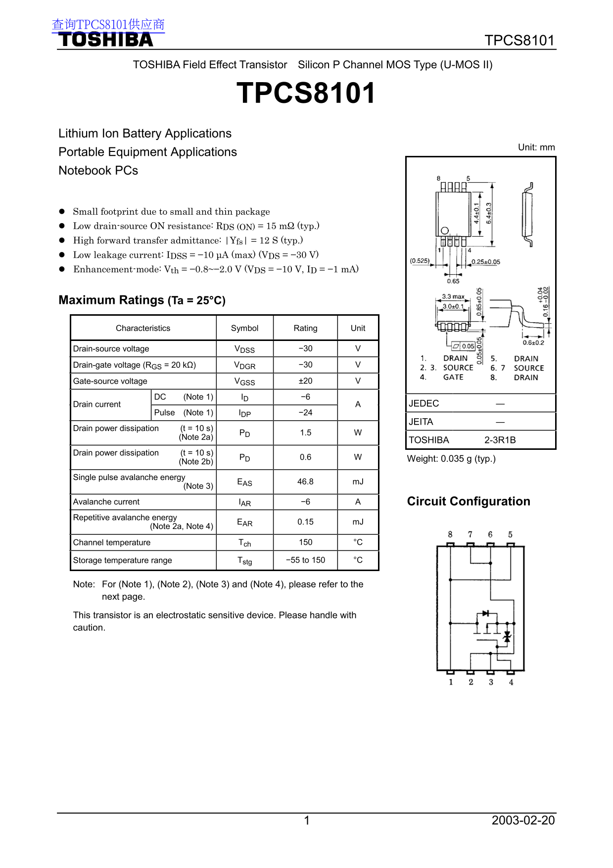
Page 1 Text Content
查询TPCS8101供应商
TPCS8101
TOSHIBA Field Effect Transistor Silicon P Channel MOS Type (U-MOS II)
TPCS8101
Lithium Ion Battery Applications
Unit: mm
Portable Equipment Applications Notebook PCs
Small footprint due to small and thin package Low drain-source ON resistance: RDS (ON) = 15 mΩ (typ.) High forward transfer admittance: |Yfs| = 12 S (typ.) Low leakage current: IDSS = −10 µA (max) (VDS = −30 V) Enhancement-mode: Vth = −0.8~−2.0 V (VDS = −10 V, ID = −1 m A)
Maximum Ratings (Ta = 25°C)
Characteristics Symbol Rating Unit
Drain-source voltage VDSS −30 V Drain-gate voltage (RGS = 20 kΩ) VDGR −30 V Gate-source voltage VGSS ±20 V
DC (Note 1) ID −6
Drain current JEDEC ―
Pulse (Note 1) IDP −24
JEITA ―
Drain power dissipation (t = 10 s) (Note 2a) PD 1.5 W
TOSHIBA 2-3R1B
Drain power dissipation (t = 10 s)
Weight: 0.035 g (typ.)
(Note 2b) PD 0.6 W Single pulse avalanche energy (Note 3) EAS 46.8 m J Avalanche current IAR −6 A Circuit Configuration Repetitive avalanche energy (Note 2a, Note 4) EAR 0.15 m J Channel temperature Tch 150 °C
Storage temperature range Tstg −55 to 150 °C
Note: For (Note 1), (Note 2), (Note 3) and (Note 4), please refer to the next page.
This transistor is an electrostatic sensitive device. Please handle with caution.
Page Summary Contents For Toshiba TPCS8101 Data Handbook
Manual Details
| Brand | Toshiba |
|---|---|
| Pages | 7 |
| File Size | 310.79 KB |
| Published | July 22, 2026 |
Enter the captcha to get the download link:

Frequently Asked Questions
What is the maximum drain-source voltage for this transistor?
The maximum drain-source voltage ($V_{DSS}$) rating is -30 V.
Are there specific handling precautions I must follow?
Yes, note that this transistor is an electrostatic sensitive device and requires careful handling.
What are the usage restrictions regarding life-critical applications?
These products are not intended for use in equipment where failure could cause loss of human life, such as medical instruments or aircraft systems.
How must I manage the operating temperature when installing it?
The channel temperature ($T_{ch}$) must be kept below 150 °C during operation.