Toshiba TC7SH125FS User Guide
Summary
This high-performance Toshiba CMOS Bus Buffer (TC7SH125FS) is designed for reliable signal conditioning in digital logic circuits. It features ultra-high speed and low power dissipation across a wide operating voltage range of 2 to 5.5V, making it ideal for data bus applications. The comprehensive datasheet outlines critical specifications, including absolute maximum ratings, detailed DC/AC electrical parameters (e.g., propagation delays), pin assignments in the SON5-P-0.35 package, and logic truth tables. This document serves engineers and design professionals selecting components for high-speed digital system development.
Page 1 Text Content
TC7SH125FS
TOSHIBA CMOS Digital Integrated Circuit Silicon Monolithic
TC7SH125FS
Bus Buffer with 3-STATE Output
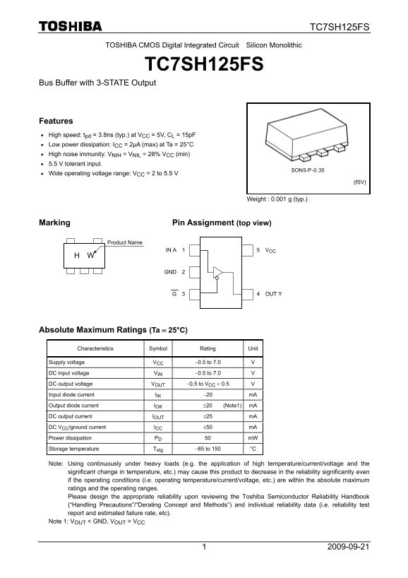
Features • High speed: tpd = 3.8ns (typ.) at VCC = 5V, CL = 15p F • Low power dissipation: ICC = 2μA (max) at Ta = 25°C • High noise immunity: VNIH = VNIL = 28% VCC (min) • 5.5 V tolerant input.
SON5-P-0.35
• Wide operating voltage range: VCC = 2 to 5.5 V
(f SV)
Weight : 0.001 g (typ.)
Marking Pin Assignment (top view)
Product Name
IN A 1 5 VCC
GND 2
G 3 4 OUT Y
Absolute Maximum Ratings (Ta = 25°C)
Characteristics Symbol Rating Unit
Supply voltage VCC −0.5 to 7.0 V
DC input voltage VIN −0.5 to 7.0 V
DC output voltage VOUT −0.5 to VCC + 0.5 V
Input diode current IIK −20 m A
Output diode current IOK ±20 (Note1) m A
DC output current IOUT ±25 m A
DC VCC/ground current ICC ±50 m A
Power dissipation PD 50 m W
Storage temperature Tstg −65 to 150 °C
Note: Using continuously under heavy loads (e.g. the application of high temperature/current/voltage and the significant change in temperature, etc.) may cause this product to decrease in the reliability significantly even if the operating conditions (i.e. operating temperature/current/voltage, etc.) are within the absolute maximum ratings and the operating ranges. Please design the appropriate reliability upon reviewing the Toshiba Semiconductor Reliability Handbook (“Handling Precautions”/“Derating Concept and Methods”) and individual reliability data (i.e. reliability test report and estimated failure rate, etc). Note 1: VOUT < GND, VOUT > VCC
Page Summary Contents For Toshiba TC7SH125FS User Guide
Manual Details
| Brand | Toshiba |
|---|---|
| Pages | 6 |
| File Size | 177.86 KB |
| Published | June 15, 2026 |
Enter the captcha to get the download link:

Frequently Asked Questions
What is the acceptable operating voltage range for VCC?
The specified operating voltage window for VCC is between 2.0 to 5.5 V.
How should I calculate average power dissipation?
Use the formula: I = C × V × f + I_CC (opr).
What are the operational temperature limits?
The product is rated for an operating temperature range of -40 to 85°C.
Are there precautions regarding reliability under stress?
Continuous heavy loads or significant temp/current changes can degrade reliability, requiring review against the Toshiba Handbook.