Toshiba TC7SH125FS Data Handbook
Summary
Enhance your circuit integrity with the TC7SH125FS CMOS Bus Buffer digital integrated circuit. This high-speed component offers superior signal buffering capabilities, defined by its low power dissipation and wide operating voltage range (2V–5.5V). The accompanying documentation provides comprehensive technical deep dives, including detailed AC/DC electrical characteristics, maximum ratings, and recommended usage guidelines. It is essential for electronics designers building reliable, general-purpose systems that require robust signal coupling in varied environments.
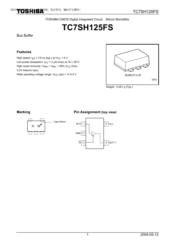
Page 1 Text Content
TC7SH125FS
TOSHIBA CMOS Digital Integrated Circuit Silicon Monolithic
TC7SH125FS
Bus Buffer
Features High speed: tpd = 3.8 ns (typ.) at VCC = 5 V Low power dissipation: ICC = 2 µA (max) at Ta = 25°C High noise immunity: VNIH = VNIL = 28% VCC (min) 5.5V tolerant input. Wide operating voltage range: VCC (opr) = 2~5.5 V
SON5-P-0.35
(f SV)
Weight : 0.001 g (Typ.)
Marking Pin Assignment (top view)
Type Name
IN A VCC
OUT Y
Page Summary Contents For Toshiba TC7SH125FS Data Handbook
Manual Details
| Brand | Toshiba |
|---|---|
| Pages | 6 |
| File Size | 140.71 KB |
| Published | June 06, 2026 |
Enter the captcha to get the download link:

Frequently Asked Questions
What is the recommended operating temperature range for this device?
The product operates between -40°C and 85°C.
What are the typical high speed specifications for TC7SH125FS?
It boasts a high speed of t = 3.8 ns (typ.) at V = 5 V.
Can this device handle various voltage levels?
Yes, it has a wide operating voltage range from 2V to 5.5V.
Are there specific guidelines against using the product?
The device is not intended for critical applications like medical or aviation instruments due to safety risks.