# A B C D E F G H I J K L M N O P Q R S T U V W X Y Z

Texas Instruments VSP3200 VSP3210 Data Sheet

Summary

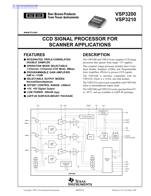
The VSP3200 and VSP3210 are complete CCD signal processors featuring triple-correlated double samplers and programmable gain amplifiers. Optimized for scanner applications, these CMOS-compatible chips support 1- or 3-channel operation up to 8Msps and operate on single +5V supplies.
📄 Preview PAGE OF 16

Page 1 Text Content

查询VSP3200供应商

VSP3200

VSP3200 VSP3210

www.ti.com

CCD SIGNAL PROCESSOR FOR SCANNER APPLICATIONS FEATURES DESCRIPTION

INTEGRATED TRIPLE-CORRELATED The VSP3200 and VSP3210 are complete CCD image DOUBLE SAMPLER processors that operate from single +5V supplies. OPERATION MODE SELECTABLE: This complete image processor includes three Corre- 1-Channel, 3-Channel CCD Mode, 8Msps lated Double Samplers (CDSs) and Programmable

PROGRAMMABLE GAIN AMPLIFIER: Gain Amplifiers (PGAs) to process CCD signals.

0d B to +13d B The VSP3200 is interface compatible with the SELECTABLE OUTPUT MODES: VSP3210, which is a 16-bit, one-chip product. Normal/Demultiplexed

The VSP3210 is pin-to-pin compatible with VSP3100,

OFFSET CONTROL RANGE: ±500m V when in demultiplexed output mode. +3V, +5V Digital Output The VSP3200 and VSP3210 can be operated from 0°C LOW POWER: 300m W (typ) to +85°C, and are available in LQFP-48 packages. LQFP-48 SURFACE-MOUNT PACKAGE

CK1CLP CK2 ADCCK VREFTP0

Reference

Circuit

Timing Generator

Clamp

CDS PGA REFN

10-Bit OE

DAC VDRV

Clamp

GINP 16-Bit Digital

CDS PGA MUX A/D Output

Converter Control

10-Bit DAC

Clamp

CDS PGA

Gain Offset Control

10-Bit

Register Register Register

Configuration

Register WRT RD SCLK SD

VSP3200

Copyright © 2000, Texas Instruments Incorporated SBMS012A Printed in U.S.A. November, 2000

Page Summary Contents For Texas Instruments VSP3200 VSP3210 Data Sheet

Page 1 查询VSP3200供应商 VSP3200 VSP3200 VSP3210 www.ti.com CCD SIGNAL PROCESSOR FOR SCANNER APPLICATIONS FEATURES DESCRIPTION INTEGRATED TRIPLE-CORRELATED The VSP3200 and VSP3210 are complete CCD image DOUBLE SA...
Page 2 SPECIFICATIONS At TA = 25°C, VCC = +5.0V, VDRV = +3.0V, Conversion Rate (f ADCCK) = 6MHz, f CK1 = 2MHz, f CK2 = 2MHz, PGA Gain = 1, normal output mode, no output load, unless otherwise specified. VSP3...
Page 3 ABSOLUTE MAXIMUM RATINGS(1) ELECTROSTATIC Supply Voltage: VCC, VDRV +6.5V Supply Voltage Differences: Among VCC ±0.1V DISCHARGE SENSITIVITY GND Voltage Differences: Among GNDA ±0.1V Digital Input Volt...
Page 4 PIN CONFIGURATION Top View LQFP B12 (A2) OE B13 VCC B14 SCLK B15 (MSB) SD VDRV P/S VCC WRT VSP3200Y 0) VCC RD AGND AGND TP0 CK2 IN (D 7) VREF CK1 VCC ADCCK IN (D 5) REFN VCC IN (D 3) LP (D 0) PIN DESC...
Page 5 PIN CONFIGURATION Top View LQFP B6, B14 OE B7, B15 (MSB) VCC NC SCLK NC SD VDRV AGND VCC WRT VSP3210Y VCC AGND AGND AGND TP0 CK2 VREF CK1 VCC ADCCK REFN VCC IN 1, PIN DESCRIPTIONS (VSP3210Y) PIN DESIG...
Page 6 TIMING SPECIFICATIONS VSP3200 AND VSP3210 1-CHANNEL CCD MODE TIMING Pixel 1 Pixel 2 CCD Output t CK1W-1 t CK1P-1 t CK2W-1 t CK1CK2-1 t CK2CK1-1 t CK1ADC t CNV t SET t ADCCK2-1 ADCCK Pixel 1 t ADCW t A...
Page 7 VSP3200 AND VSP 3210 3-CHANNEL CCD MODE TIMING Pixel 1 (R/G/B) Pixel 2 (R/G/B) CCD Output t St S t CK1W-3 t CK1P-3 t CK2W-3 t CK1CK2-3 t SET t CK2CK1-3 t SET t ADCCK2-3 t CNV ADCCK (R) (G) (B) Pixel 1...
Page 8 DIGITAL DATA OUTPUT SEQUENCE: 1-Ch CCD Mode, (B-Ch: D4 = 1 and D5 = 0) Pixel (n) Pixel (n+1) Pixel (n+8) CCD Output CK1 • • • t SET t SET CK2 • • • t CNV t CNV ADCCK CDS Output (n) (n+1) • • • (n+7) (...
Page 9 VSP3200 AND VSP3210 TIMING FOR DIGITAL DATA OUT- VSP3200 TIMING FOR DIGITAL DATA OUTPUT PUT (DEMULTIPLEXED OUTPUT MODE) (NORMAL OUTPUT MODE) t OES t OEP t OES t OEP t OEW t OEW OE OE t OER t3E t OER t...
Page 10 3-CHANNEL CCD MODE THEORY OF OPERATION In the 3-Channel CCD mode, the VSP3200 and VSP3210 can INTRODUCTION simultaneously process triple output CCD signals. CCD sig- The VSP3200 and VSP3210 are comple...
Page 11 The VSP3210 can be operated in Demultiplexed mode as the VSP3200 and VSP3210 from any digital noise activities on digital output (B13-based Big Endian Format), as shown in the bus coupling back high-f...
Page 12 INPUT CLAMP In this equivalent circuit, Input Coupling Capacitor CIN, and Sampling Capacitor C1, are constructed as a capacitor divider The input clamp should be used for 1-Channel and 3-Channel durin...
Page 13 other system circuits, as it would affect the reference OE P/S MODE voltage of the A/D converter and prevent proper A/D Digital data output enabled, Serial mode enabled conversion. Prohibit mode (can ...
Page 14 OFFSET REGISTER RECOMMENDATION FOR POWER SUPPLY, Offset Registers control the analog offset input to channels GROUNDING, AND DEVICE DECOUPLING prior to the PGA. There is a 10-bit Offset Register on ea...
Page 15 PACKAGE DRAWING MPQF102
Page 16 IMPORTANT NOTICE Texas Instruments Incorporated and its subsidiaries (TI) reserve the right to make corrections, modifications, enhancements, improvements, and other changes to its products and servic...

Manual Details

Brand Texas Instruments
Pages 16
File Size 339.73 KB
Published June 15, 2026
4 views

Enter the captcha to get the download link:

captcha

Frequently Asked Questions

What is the maximum conversion rate?

8 MHz in both 1-channel and 3-channel CCD mode.

What is the offset control range?

±500 mV via a 10-bit control DAC.

Is the VSP3210 pin-compatible with the VSP3100?

Yes, the VSP3210 is pin-to-pin compatible with the VSP3100 when operated in demultiplexed output mode.

What is the operating temperature range?

0°C to +85°C.