Texas Instruments CDC2586 Data Sheet
Summary
The CDC2586 is a high-performance, low-skew 3.3V phase-lock loop clock driver designed for critical synchronization in digital systems. It precisely distributes one clock input signal to twelve outputs using an advanced PLL, ensuring minimal jitter and maximum signal integrity for demanding applications. Ideal for networking synchronous DRAM or modern microprocessors operating at speeds up to 100 MHz. This comprehensive documentation details the device’s internal architecture, including selectable output configurations (half or double frequency), low-power operation, and best practices for achieving phase lock in high-speed digital designs.
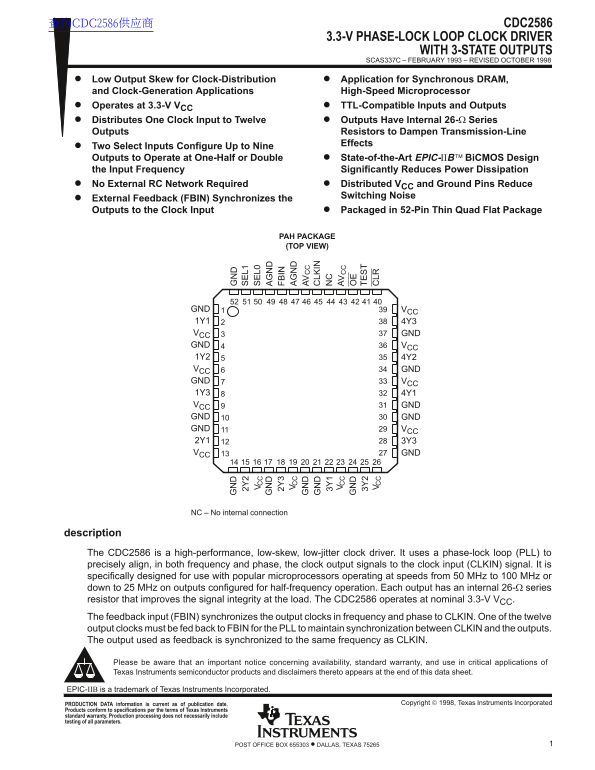
Page 1 Text Content
查询CDC2586供应商 CDC2586
3.3-V PHASE-LOCK LOOP CLOCK DRIVER
WITH 3-STATE OUTPUTS SCAS337C – FEBRUARY 1993 – REVISED OCTOBER 1998
Low Output Skew for Clock-Distribution Application for Synchronous DRAM, and Clock-Generation Applications High-Speed Microprocessor Operates at 3.3-V VCC TTL-Compatible Inputs and Outputs Distributes One Clock Input to Twelve Outputs Have Internal 26-Ω Series Outputs Resistors to Dampen Transmission-Line
Effects
Two Select Inputs Configure Up to Nine Outputs to Operate at One-Half or Double State-of-the-Art EPIC-ΙΙB Bi CMOS Design the Input Frequency Significantly Reduces Power Dissipation No External RC Network Required Distributed VCC and Ground Pins Reduce
Switching Noise
External Feedback (FBIN) Synchronizes the Outputs to the Clock Input Packaged in 52-Pin Thin Quad Flat Package
PAH PACKAGE
2Y (TOP VIEW) L1 L0
2Y IN
GND VCC
LK IN
VCC GND
GND VCC 1Y2 4Y2
VCC GND
GND VCC 1Y3 4Y1 VCC GND GND GND GND VCC 2Y1 3Y3 VCC GND
NC – No internal connection
description The CDC2586 is a high-performance, low-skew, low-jitter clock driver. It uses a phase-lock loop (PLL) to precisely align, in both frequency and phase, the clock output signals to the clock input (CLKIN) signal. It is specifically designed for use with popular microprocessors operating at speeds from 50 MHz to 100 MHz or down to 25 MHz on outputs configured for half-frequency operation. Each output has an internal 26-Ω series resistor that improves the signal integrity at the load. The CDC2586 operates at nominal 3.3-V VCC. The feedback input (FBIN) synchronizes the output clocks in frequency and phase to CLKIN. One of the twelve output clocks must be fed back to FBIN for the PLL to maintain synchronization between CLKIN and the outputs. The output used as feedback is synchronized to the same frequency as CLKIN.
Please be aware that an important notice concerning availability, standard warranty, and use in critical applications of Texas Instruments semiconductor products and disclaimers thereto appears at the end of this data sheet.
EPIC-ΙΙΒ is a trademark of Texas Instruments Incorporated.
Copyright 1998, Texas Instruments Incorporated PRODUCTION DATA information is current as of publication date.
Products conform to specifications per the terms of Texas Instruments standard warranty. Production processing does not necessarily include testing of all parameters.
1POST OFFICE BOX 655303 • DALLAS, TEXAS 75265
Page Summary Contents For Texas Instruments CDC2586 Data Sheet
Manual Details
| Brand | Texas Instruments |
|---|---|
| Pages | 12 |
| File Size | 149.34 KB |
| Published | June 02, 2026 |
Enter the captcha to get the download link:

Frequently Asked Questions
What is the operating voltage for the CDC2586?
The device operates at a nominal 3.3-V V CC.
Does the CDC2586 require external components like an RC network?
No, the CDC2586 does not require external RC networks because the loop filter for the PLL is included on-chip.
How can I change the output frequency of the Y outputs?
Select inputs (SEL1, SEL0) configure up to nine Y outputs to operate at one-half or double the CLKIN frequency depending on which output is fed back to FBIN.
When should I consider stabilization time?
Stabilization time is required after power up and application of a fixed-frequency signal, as well as when changing PLL reference/feedback signals or enabling outputs via OE.