Texas Instruments TRF1223 Data Sheet
Summary
Texas Instruments TRF1223 product datasheet describing a 3.3-GHz to 3.8-GHz 1-watt linear power amplifier MMIC for transmitter applications. Features include 30 dB gain, two TTL-controlled 16-dB gain steps for 32 dB total gain control, temperature-compensated detector, auto-bias design, and internally matched 50-ohm input/output. Intended for RF engineers designing 3.5 GHz wireless communication systems using complex modulation schemes such as QAM or OFDM.
Page 1 Text Content
查询TRF1223供应商
TRF1223
www.ti.com
SLWS166A–APRIL 2005–REVISED JULY
3.3-GHz TO 3.8-GHZ 1-W Power Amplifier
FEATURES
VPOS VNEG
P-1d B Linear, 30-d B Gain Transmitter Operates Over the 3300-MHz to 3800-MHz
Power
Range
PACNT
Supply VDD
Two TTL Controlled, 1-bit, 16-d B Gain Steps LP
for d B of Total Gain Control
Power Amp / Driver
Pre-Amp
Superior Linearity (+45 d Bm IP3) Over the Attenuator Amplifier
Entire Frequency Range RFO RFI Auto-Bias Design With PA Enable Temperature Compensated Directional Coupler Detector DETN
Low Power Bias Mode Internally Matched 50-Ω Input and Output
PAGAIN1 PAGAIN0
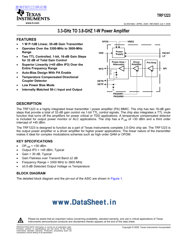
DESCRIPTION The TRF1223 is highly integrated linear transmitter power amplifier (PA) MMIC. The chip has two 16-d B gain steps that provide total of 32-d B gain control via 1-bit TTL control signals. The chip also integrates TTL mute function that turns off the amplifiers for power critical or TDD applications. temperature compensated detector is included for output power monitor or ALC applications. The chip has P1d B of +30 d Bm and third order intercept of +45 d Bm. The TRF1223 is designed to function as part of Texas Instruments complete 3.5-GHz chip set. The TRF1223 is the output power amplifier or driver amplifier for higher power applications. The linear nature of the transmitter makes it ideal for complex modulations schemes such as high order QAM or OFDM.
KEY SPECIFICATIONS OP1d B +30 d Bm Output IP3 +45 d Bm, Typical Gain d B, Typical Gain Flatness over Transmit Band ±2 d B Frequency Range MHz to MHz ±0.5-d B Detected Output Voltage vs Temperature
BLOCK DIAGRAM The detailed block diagram and the pin-out of the ASIC are shown in Figure 1.
Please be aware that an important notice concerning availability, standard warranty, and use in critical applications of Texas Instruments semiconductor products and disclaimers thereto appears at the end of this data sheet.
PRODUCTION DATA information is current as of publication date. Copyright 2005, Texas Instruments Incorporated Products conform to specifications per the terms of the Texas Instruments standard warranty. Production processing does not necessarily include testing of all parameters.
Page Summary Contents For Texas Instruments TRF1223 Data Sheet
Manual Details
| Brand | Texas Instruments |
|---|---|
| Pages | 10 |
| File Size | 124.53 KB |
| Published | June 17, 2026 |
Enter the captcha to get the download link:

Frequently Asked Questions
What is the operating frequency range of TRF1223?
It operates over 3300 MHz to 3800 MHz.
What is the proper power up sequence for TRF1223?
Power up VNEG first, then VPOS, then VDD.
How is total gain control achieved on TRF1223?
Via two 1-bit TTL gain steps, each 16 dB, total 32 dB.
What ESD precautions are needed for TRF1223?
Use protective garments, ESD work areas, shielded containers, and treat it as ESD sensitive.