Texas Instruments TPS786xx Data Sheet
Summary
The TPS786xx family provides high-performance Low-Dropout (LDO) linear regulators engineered for sensitive analog electronics. This series guarantees ultra-low noise, high Power Supply Rejection Ratio (PSRR), and excellent transient response in compact packages. The documentation guides designers on implementing this robust voltage solution for mission-critical applications, including RF circuitry (VCOs, ADCs), audio systems, Bluetooth/Wi-Fi devices, and portable cellular electronics requiring stable power delivery.
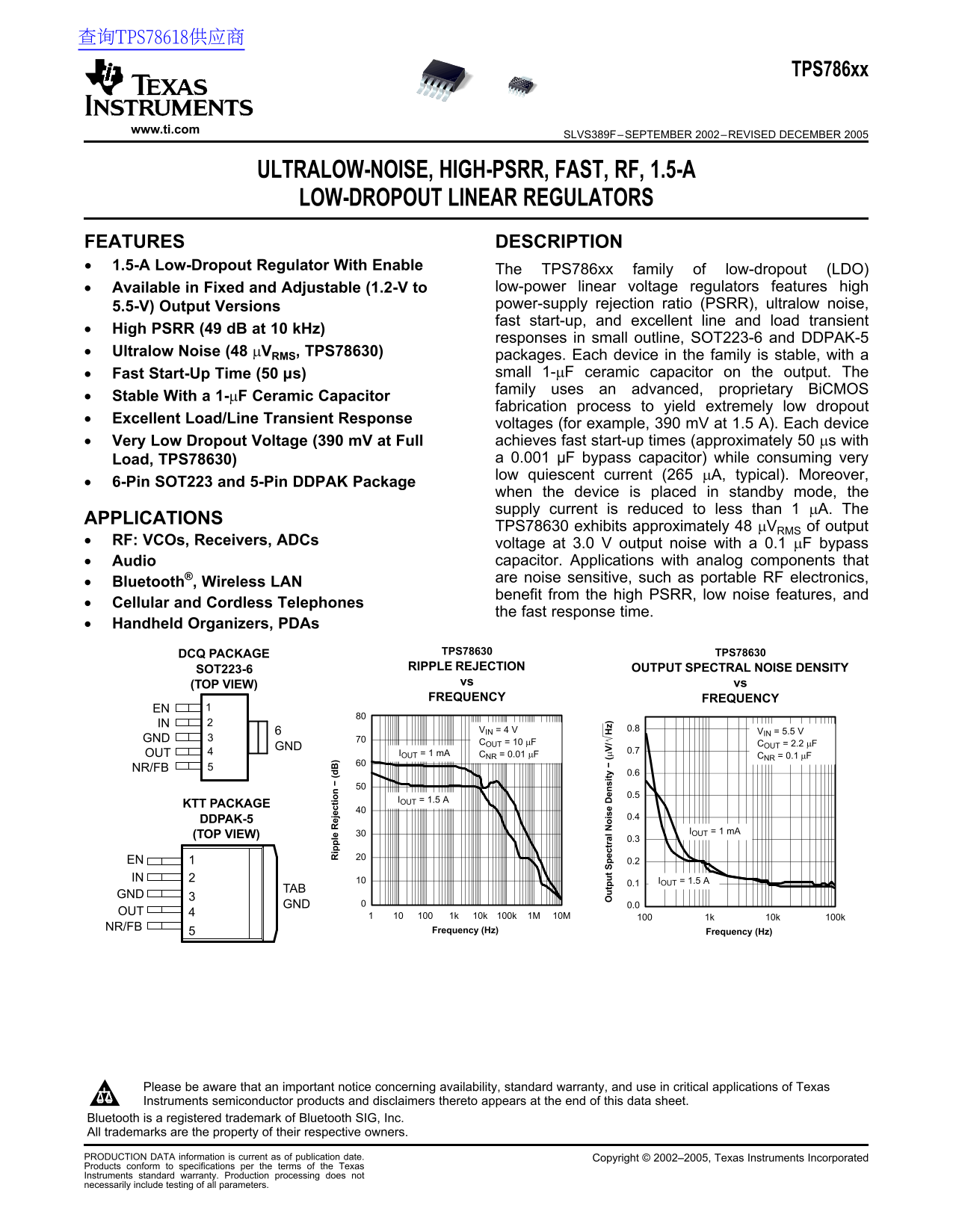
Page 1 Text Content
查询TPS78618供应商
TPS786xx
www.ti.com
SLVS389F–SEPTEMBER 2002–REVISED DECEMBER
ULTRALOW-NOISE, HIGH-PSRR, FAST, RF, 1.5-A
LOW-DROPOUT LINEAR REGULATORS
FEATURES DESCRIPTION
1.5-A Low-Dropout Regulator With Enable
The TPS786xx family of low-dropout (LDO)
Available in Fixed and Adjustable (1.2-V to low-power linear voltage regulators features high•
Output Versions power-supply rejection ratio (PSRR), ultralow noise,5.5-V)
fast start-up, and excellent line and load transient•
High PSRR (49 d B at k Hz)
ip le ej ec ti
responses in small outline, SOT223-6 and DDPAK-5
Ultralow Noise (48 µVRMS, TPS78630)
packages. Each device in the family is stable, with
Fast Start-Up Time (50 µs) small 1-µF ceramic capacitor on the output. The•
family uses an advanced, proprietary Bi CMOS•
Stable With 1-µF Ceramic Capacitor
fabrication process to yield extremely low dropout
Excellent Load/Line Transient Response
voltages (for example, m V at 1.5 A). Each device
Very Low Dropout Voltage (390 m V at Full achieves fast start-up times (approximately µs with•
TPS78630) 0.001 µF bypass capacitor) while consuming very Load,
low quiescent current (265 µA, typical). Moreover,•
6-Pin SOT223 and 5-Pin DDPAK Package
when the device is placed in standby mode, the
supply current is reduced to less than µA. The
APPLICATIONS
TPS78630 exhibits approximately µVRMS of output
RF: VCOs, Receivers, ADCs
voltage at 3.0 output noise with 0.1 µF bypass
Audio capacitor. Applications with analog components that•
are noise sensitive, such as portable RF electronics,•
Bluetooth®, Wireless LAN
benefit from the high PSRR, low noise features, and•
Cellular and Cordless Telephones
tp ec tr al is en si ty µV z)
the fast response time.
Handheld Organizers, PDAs
DCQ PACKAGE TPS78630 TPS78630 SOT223-6 RIPPLE REJECTION OUTPUT SPECTRAL NOISE DENSITY (TOP VIEW) vs vs FREQUENCY FREQUENCY
EN IN
VIN = 4 V 0.8 VIN = 5.5 V
GND COUT = 10 µF
COUT = 2.2 µF
IOUT = 1 m A 0.7
OUT CNR = 0.01 µF CNR = 0.1 µF NR/FB
IOUT = 1.5 A
KTT PACKAGE
DDPAK-5
IOUT = 1 m A
(TOP VIEW)
EN 0.2 IN IOUT = 1.5 A
GND 0.0
NR/FB Frequency (Hz)
Frequency (Hz)
Please be aware that an important notice concerning availability, standard warranty, and use in critical applications of Texas
Instruments semiconductor products and disclaimers thereto appears at the end of this data sheet.
Bluetooth is registered trademark of Bluetooth SIG, Inc.
All trademarks are the property of their respective owners.
PRODUCTION DATA information is current as of publication date. Copyright 2002–2005, Texas Instruments Incorporated
Products conform to specifications per the terms of the Texas
Instruments standard warranty. Production processing does not
necessarily include testing of all parameters.
Page Summary Contents For Texas Instruments TPS786xx Data Sheet
Manual Details
| Brand | Texas Instruments |
|---|---|
| Pages | 18 |
| File Size | 542.38 KB |
| Published | July 16, 2026 |
Enter the captcha to get the download link:

Frequently Asked Questions
What is the typical output noise of the TPS78630?
The TPS78630 exhibits approximately 48 μV of output RMS voltage at 3.0 V.
What external components are required for stable operation?
Each device in the family is stable using a small 1-μF ceramic capacitor on the output.
How does the TPS786xx series handle standby power consumption?
In standby mode when placed in a 6-Pin SOT223 or 5-Pin DDPAK package, the supply current reduces to less than 1 μA.
What is the fast start-up time capability of this regulator family?
The family achieves fast start-up times of approximately 50 µs with a 0.001µF bypass capacitor.