# A B C D E F G H I J K L M N O P Q R S T U V W X Y Z

Texas Instruments TPS54073 Data Sheet

Summary

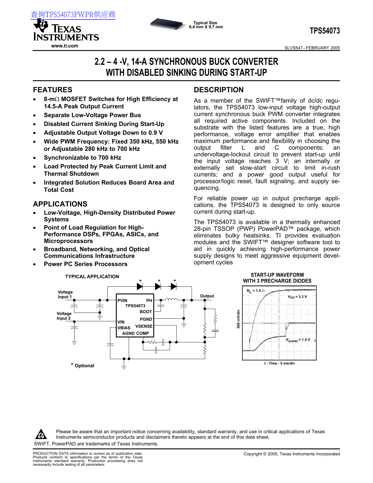
The TPS54073 is a highly efficient synchronous buck converter engineered for reliable Point of Load (PoL) regulation in modern digital power architectures. This integrated solution combines multiple switching and control features into a compact design, simplifying complex high-density power supply requirements. The manual provides comprehensive specifications covering adjustable output voltage, fast start-up sequencing, and sophisticated protection mechanisms. It is essential reading for electronics engineers designing demanding broadband, networking, or optical communication infrastructure that uses ASICs, FPGAs, and DSPs requiring robust, high-performance power delivery.
📄 Preview PAGE OF 24

Page 1 Text Content

查询TPS54073PWPR供应商

Typical Size 6,4 mm X 9,7 mm

TPS54073

www.ti.com

SLVS547–FEBRUARY

2.2 -V, 14-A SYNCHRONOUS BUCK CONVERTER

WITH DISABLED SINKING DURING START-UP

FEATURES DESCRIPTION

8-mΩ MOSFET Switches for High Efficiency at

As member of the SWIFT™family of dc/dc regu-

14.5-A Peak Output Current lators, the TPS54073 low-input voltage high-output

Separate Low-Voltage Power Bus current synchronous buck PWM converter integrates•

all required active components. Included on the•

Disabled Current Sinking During Start-Up

substrate with the listed features are true, high

Adjustable Output Voltage Down to 0.9

performance, voltage error amplifier that enables

Wide PWM Frequency: Fixed k Hz, k Hz maximum performance and flexibility in choosing the•

output filter and components; anor

Adjustable k Hz to k Hz

undervoltage-lockout circuit to prevent start-up until•

Synchronizable to k Hz

the input voltage reaches V; an internally or

Load Protected by Peak Current Limit and

externally set slow-start circuit to limit in-rush

Thermal Shutdown currents; and power good output useful for

processor/logic reset, fault signaling, and supply se-•

Integrated Solution Reduces Board Area and

quencing.Total

For reliable power up in output precharge appli-

APPLICATIONS cations, the TPS54073 is designed to only source

Low-Voltage, High-Density Distributed Power current during start-up.•

Systems

The TPS54073 is available in thermally enhanced

Point of Load Regulation for High-

28-pin TSSOP (PWP) Power PAD™ package, which

Performance DSPs, FPGAs, ASICs, and

eliminates bulky heatsinks. TI provides evaluation

/d iv

Microprocessors

modules and the SWIFT™ designer software tool to

Broadband, Networking, and Optical aid in quickly achieving high-performance power•

Infrastructure supply designs to meet aggressive equipment devel-Communications

opment cycles•

Power PC Series Processors

START-UP WAVEFORM

TYPICAL APPLICATION

WITH 3 PRECHARGE DIODES

Voltage

Input 1 Output VI/O = 3.3 V

PVIN PH TPS54073

Voltage Input 2 PGND

VSENSE

VBIAS

COMPAGND

= 1.5 V(core)

t - Time - 5 ms/div

Optional

Please be aware that an important notice concerning availability, standard warranty, and use in critical applications of Texas

Instruments semiconductor products and disclaimers thereto appears at the end of this data sheet.

SWIFT, Power PAD are trademarks of Texas Instruments.

PRODUCTION DATA information is current as of publication date. Copyright 2005, Texas Instruments Incorporated

Products conform to specifications per the terms of the Texas

Instruments standard warranty. Production processing does not

necessarily include testing of all parameters.

Page Summary Contents For Texas Instruments TPS54073 Data Sheet

Page 1 查询TPS54073PWPR供应商 Typical Size 6,4 mm X 9,7 mm TPS54073 www.ti.com SLVS547–FEBRUARY 2.2 -V, 14-A SYNCHRONOUS BUCK CONVERTER WITH DISABLED SINKING DURING START-UP FEATURES DESCRIPTION 8-mΩ MOSFET Switc...
Page 2 TPS54073 www.ti.com SLVS547–FEBRUARY These devices have limited built-in ESD protection. The leads should be shorted together or the device placed in conductive foam during storage or handling to prev...
Page 3 TPS54073 www.ti.com SLVS547–FEBRUARY DISSIPATION RATINGS (continued) THERMAL IMPEDANCE TA 25°C TA 70°C TA 85°CPACKAGE JUNCTION-TO-AMBIENT POWER RATING POWER RATING POWER RATING 28-Pin PWP without sold...
Page 4 TPS54073 www.ti.com SLVS547–FEBRUARY ELECTRICAL CHARACTERISTICS (continued) TJ -40°C to 125°C, VIN to V, PVIN 2.2 to (unless otherwise noted) PARAMETER TEST CONDITIONS MIN TYP MAX UNIT ERROR AMPLIFIER...
Page 5 TPS54073 www.ti.com SLVS547–FEBRUARY DEVICE INFORMATION PWP PACKAGE (TOP VIEW) AGND RT VSENSE SYNC COMP SS/ENA PWRGD VBIAS BOOT VIN PH PVIN PH THERMAL PVIN PH PVIN PH PVIN PH PGND PH PGND PH PGND PH P...
Page 6 TPS54073 www.ti.com SLVS547–FEBRUARY FUNCTIONAL BLOCK DIAGRAM AGND VBIAS VIN VIN REGVBIAS 3.0 − 4.0 V Enable Comparator SS/ENA Falling SHUTDOWN Edge ILIM PVIN Deglitch 2.2 − 4.0 V Thermal Comparator H...
Page 7 TPS54073 www.ti.com tp Vo lt ag eg la ti xt er al ly et sc ill at re en cy SLVS547–FEBRUARY ra in -S rc -S ta te is ta TYPICAL CHARACTERISTICS DRAIN-SOURCE ON-STATE DRAIN-SOURCE ON-STATE INTERNALLY SE...
Page 8 TPS54073 www.ti.com SLVS547–FEBRUARY APPLICATION INFORMATION PCB LAYOUT OPTIONAL PRE-CHARGE DIODES CONNECT TO PRE-CHARGE VOLTAGE SOURCE ANALOG GROUND TRACE FREQUENCY SET RESISTOR AGND RT VSENSE SYNC S...
Page 9 TPS54073 www.ti.com SLVS547–FEBRUARY output filter capacitor(s) between the VOUT trace and For operation at full rated load current, the analog PGND. It is important to keep the loop formed by the gro...
Page 10 TPS54073 www.ti.com SLVS547–FEBRUARY Connect to Optional Precharge Voltage Figure 12. Application Circuit, 3.3 to 1.5 Figure shows the schematic for typical TPS54073 application. The TPS54073 provides...
Page 11 TPS54073 www.ti.com SLVS547–FEBRUARY SWITCHING FREQUENCY for V, and the ripple current capacity is greater than at the operating frequency of k Hz. Total The switching frequency can be set to either o...
Page 12 TPS54073 www.ti.com SLVS547–FEBRUARY OUT IN(MAX) OUT VOUT VPVIN(MAX) VOUT I= L(PK) 1.6 Fsw x OUT(MAX) 0.8 ICOUT(RMS) IN(MAX) OUT VPVIN(MAX) LOUT Fsw (9)For this design, the RMS inductor current is 14....
Page 13 TPS54073 www.ti.com SLVS547–FEBRUARY of the switching frequency, and the phase margin at ´´ fff Z2Z1CO crossover must be greater than degrees. The general procedure outlined here produces results LCIN...
Page 14 TPS54073 www.ti.com SLVS547–FEBRUARY BIAS AND BOOTSTRAP CAPACITORS SNUBBER CIRCUIT Every TPS54073 design requires bootstrap capaci- R8 and C14 of the application schematic comprise tor, C3, and bias c...
Page 15 TPS54073 www.ti.com ff ic ie SLVS547–FEBRUARY PERFORMANCE GRAPHS The performance data for Figure through Figure are for the circuit in Figure 12. Conditions are PVIN 2.5 V, VIN 3.3 V, VO 1.5 V, fs k H...
Page 16 TPS54073 www.ti.com SLVS547–FEBRUARY PERFORMANCE GRAPHS (continued) The performance data for Figure through Figure are for the circuit in Figure 13. Conditions are PVIN VIN 3.3 V, VO 1.5 V, fs k Hz, a...
Page 17 TPS54073 www.ti.com SLVS547–FEBRUARY DETAILED DESCRIPTION PVIN and VIN can be tied together for 3.3-V bus operation. OPERATING WITH SEPARATE PVIN MAXIMUM OUTPUT VOLTAGE The TPS54073 is designed to ope...
Page 18 TPS54073 www.ti.com SLVS547–FEBRUARY SLOW-START/ENABLE (SS/ENA) or digital-switching noise may degrade performance. The VBIAS pin may be useful as reference voltage The slow-start/enable pin provides ...
Page 19 TPS54073 www.ti.com SLVS547–FEBRUARY remains on until the next oscillator pulse discharges OVERCURRENT PROTECTION the PWM ramp. During transient conditions, the error The cycle-by-cycle current limiti...
Page 21 PACKAGE OPTION ADDENDUM www.ti.com 19-May-2005 PACKAGING INFORMATION Orderable Device Status Package Package Pins Package Eco Plan Lead/Ball Finish MSL Peak Temp Type Drawing Qty TPS54073PWP ACTIVE HT...
Page 23 IMPORTANT NOTICE Texas Instruments Incorporated and its subsidiaries (TI) reserve the right to make corrections, modifications, enhancements, improvements, and other changes to its products and servic...
Page 24 WWW.ALLDATASHEET.COM Copyright © Each Manufacturing Company. All Datasheets cannot be modified without permission. This datasheet has been download from : www.All Data Sheet.com 100% Free Data Sheet S...

Manual Details

Brand Texas Instruments
Pages 24
File Size 1.54 MB
Published July 16, 2026
0 views

Enter the captcha to get the download link:

captcha

Frequently Asked Questions

What features make this synchronous buck converter integrated?

It integrates a low-voltage power bus, adjustable voltage down to 0.9V, and slow-start circuits.

How should I handle the device to avoid electrostatic damage?

Since it has limited built-in ESD protection, ensure the leads are shorted or store it in conductive foam.

Does the packaging help reduce board size and weight?

Yes, it uses a thermally enhanced 28-pin TSSOP (PWP) PowerPAD™ package to eliminate bulky heatsinks.