# A B C D E F G H I J K L M N O P Q R S T U V W X Y Z

Texas Instruments TPS40060 TPS40061 Data Sheet

Summary

The TPS40060/TPS40061 are high-reliability, wide-input synchronous buck controllers designed for advanced power management. These step-down converters efficiently operate across a 10V to 55V input range and feature programmable soft-start, UVLO, and integrated gate drivers. The manual details technical specifications, operational ranges, and anti-cross conduction circuitry. Ideal for mission-critical environments such as networking equipment, telecom base stations, and servers requiring robust power control.
📄 Preview PAGE OF 28

Page 1 Text Content

TPS40060 TPS40061

www.ti.com

SLUS543D–DECEMBER 2002–REVISED SEPTEMBER

WIDE-INPUT SYNCHRONOUS BUCK CONTROLLER

FEATURES DESCRIPTION Operating Input Voltage to

The TPS40060 and TPS40061 are high-voltage, wide Input Voltage Feed-Forward Compensation input (10 to V) synchronous, step-down con-• verters.•

1% Internal 0.7-V Reference

Programmable Fixed-Frequency, Up to 1-MHz This family of devices offers design flexibility with a• variety of user programmable functions, including;Voltage

Mode Controller

soft-start, UVLO, operating frequency, voltage

Internal Gate Drive Outputs for High-Side

feed-forward, high-side current limit, and loop com-

P-Channel and Synchronous N-Channel

pensation. These devices are also synchronizable to

MOSFETs

an external supply.

16-Pin Power PAD™ Package (θJC 2°C/W)

The TPS40060 and TPS40061 incorporate MOSFET

Thermal Shutdown gate drivers for external P-channel high-side and

Externally Synchronizable N-channel synchronous rectifier (SR) MOSFETs.• Gate drive logic incorporates anti-cross conduction•

Programmable High-Side Sense Short Circuit

circuitry to prevent simultaneous high-side and Protection synchronous rectifier conduction.

Programmable Closed-Loop Soft-Start TPS40060 Source Only/TPS40061 Source/Sink

APPLICATIONS Networking Equipment Telecom Equipment

Stations Servers

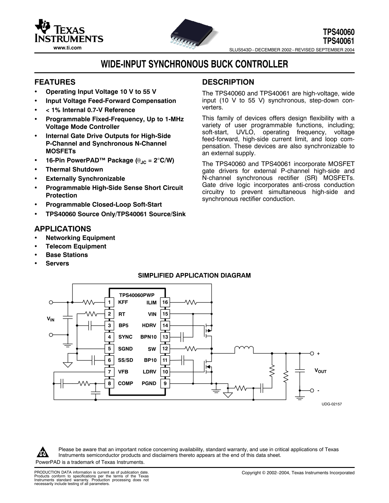
SIMPLIFIED APPLICATION DIAGRAM

TPS40060PWP KFF ILIM

RT VIN

BP5 HDRV

SYNC BPN10

SGND SW

SS/SD BP10

VFB LDRV

COMP PGND

UDG-02157

Please be aware that an important notice concerning availability, standard warranty, and use in critical applications of Texas Instruments semiconductor products and disclaimers thereto appears at the end of this data sheet.

Power PAD is trademark of Texas Instruments. PRODUCTION DATA information is current as of publication date. Copyright 2002–2004, Texas Instruments Incorporated Products conform to specifications per the terms of the Texas Instruments standard warranty. Production processing does not necessarily include testing of all parameters.

Page Summary Contents For Texas Instruments TPS40060 TPS40061 Data Sheet

Page 1 TPS40060 TPS40061 www.ti.com SLUS543D–DECEMBER 2002–REVISED SEPTEMBER WIDE-INPUT SYNCHRONOUS BUCK CONTROLLER FEATURES DESCRIPTION Operating Input Voltage to The TPS40060 and TPS40061 are high-voltage,...
Page 2 TPS40060 TPS40061 www.ti.com SLUS543D–DECEMBER 2002–REVISED SEPTEMBER These devices have limited built-in ESD protection. The leads should be shorted together or the device placed in conductive foam d...
Page 3 TPS40060 TPS40061 www.ti.com SLUS543D–DECEMBER 2002–REVISED SEPTEMBER ELECTRICAL CHARACTERISTICS TA –40°C to 85°C, VIN Vdc, RT kΩ, IKFF µA, f SW k Hz, all parameters at zero power dissipation (unless ...
Page 4 TPS40060 TPS40061 www.ti.com SLUS543D–DECEMBER 2002–REVISED SEPTEMBER ELECTRICAL CHARACTERISTICS (continued) TA –40°C to 85°C, VIN Vdc, RT kΩ, IKFF µA, f SW k Hz, all parameters at zero power dissipat...
Page 5 TPS40060 TPS40061 www.ti.com SLUS543D–DECEMBER 2002–REVISED SEPTEMBER Terminal Functions TERMINAL I/O DESCRIPTION NAME NO. 5-V reference. This pin should be bypassed to ground with 0.1-µF ceramic capa...
Page 6 TPS40060 TPS40061 www.ti.com SLUS543D–DECEMBER 2002–REVISED SEPTEMBER SIMPLIFIED BLOCK DIAGRAM BP10VIN BPN10 Clock 10−V Regulator VIN Oscillator 07VREF CL Ramp Generator 1V5REF Reference 3−bit up/down...
Page 7 TPS40060 TPS40061 www.ti.com SLUS543D–DECEMBER 2002–REVISED SEPTEMBER APPLICATION INFORMATION The TPS40060/61 family of parts allows the user to optimize the PWM controller to the specific application...
Page 8 TPS40060 TPS40061 www.ti.com SLUS543D–DECEMBER 2002–REVISED SEPTEMBER - T im in es is ta ce kΩ APPLICATION INFORMATION (continued) The PWM ramp must be faster than the master clock frequency or the PW...
Page 9 TPS40060 TPS40061 www.ti.com SLUS543D–DECEMBER 2002–REVISED SEPTEMBER APPLICATION INFORMATION (continued) RKFF VIN 3.5 65.27 RT () (min) where: VIN is the desired start-up (UVLO) input voltage RT is ...
Page 10 TPS40060 TPS40061 www.ti.com SLUS543D–DECEMBER 2002–REVISED SEPTEMBER APPLICATION INFORMATION (continued) The impedance of the input voltage can cause the input voltage, at the TPS4006x, to sag when t...
Page 11 TPS40060 TPS40061 www.ti.com SLUS543D–DECEMBER 2002–REVISED SEPTEMBER APPLICATION INFORMATION (continued) PROGRAMMING CURRENT LIMIT This device uses two-tier approach for overcurrent protection. The f...
Page 12 TPS40060 TPS40061 www.ti.com SLUS543D–DECEMBER 2002–REVISED SEPTEMBER APPLICATION INFORMATION (continued) INTERNAL REGULATOR OUTPUT VOLTAGE vs INPUT VOLTAGE tp lt ag BPN10 VIN - Input Voltage - V Figu...
Page 13 TPS40060 TPS40061 www.ti.com SLUS543D–DECEMBER 2002–REVISED SEPTEMBER APPLICATION INFORMATION (continued) CBPN10 (F) The 10-V reference pin, BP10V needs to provide energy for the synchronous MOSFET ga...
Page 14 TPS40060 TPS40061 www.ti.com SLUS543D–DECEMBER 2002–REVISED SEPTEMBER APPLICATION INFORMATION (continued) CALCULATING THE OUTPUT CAPACITANCE The output capacitance depends on the output ripple voltage...
Page 15 TPS40060 TPS40061 www.ti.com SLUS543D–DECEMBER 2002–REVISED SEPTEMBER APPLICATION INFORMATION (continued) AMOD or AMOD(db) log VIN VS VS Duty dycle, D, varies from to as the control voltage, VC, varie...
Page 16 TPS40060 TPS40061 www.ti.com SLUS543D–DECEMBER 2002–REVISED SEPTEMBER APPLICATION INFORMATION (continued) PWM MODULATOR RELATIONSHIPS MODULATOR GAIN SWITCHING FREQUENCY ESR Zero, + 1 AMOD = VIN / VS R...
Page 17 TPS40060 TPS40061 www.ti.com SLUS543D–DECEMBER 2002–REVISED SEPTEMBER APPLICATION INFORMATION (continued) The modulator gain as function of frequency at f C, is described in Equation 27. AMOD(f) AMOD...
Page 18 TPS40060 TPS40061 www.ti.com SLUS543D–DECEMBER 2002–REVISED SEPTEMBER APPLICATION INFORMATION (continued) IO ∆I BODY DIODE BODY DIODE CONDUCTION CONDUCTION ANTI-CROSS SYNCHRONOUS HIGH SIDE ON CONDUCTI...
Page 19 TPS40060 TPS40061 www.ti.com SLUS543D–DECEMBER 2002–REVISED SEPTEMBER APPLICATION INFORMATION (continued) PSR PDC PRR PCOND (W) TPS40060/TPS40061 POWER DISSIPATION The power dissipation in the TPS4006...
Page 20 TPS40060 TPS40061 www.ti.com SLUS543D–DECEMBER 2002–REVISED SEPTEMBER LAYOUT CONSIDERATIONS THE Power PAD™ PACKAGE The Power PAD package provides low thermal impedance for heat removal from the device...
Page 21 TPS40060 TPS40061 www.ti.com SLUS543D–DECEMBER 2002–REVISED SEPTEMBER DESIGN EXAMPLE Input voltage: VDC to VDC Output voltage: 3.3 ±2% Output current: (maximum, steady-state), (surge, 10-ms duration, ...
Page 22 TPS40060 TPS40061 www.ti.com SLUS543D–DECEMBER 2002–REVISED SEPTEMBER DESIGN EXAMPLE (continued) PSW(fsw) VIN IO t SW f SW ns k Hz 0.715 The MOSFET junction temperature can be found by substituting Eq...
Page 23 TPS40060 TPS40061 www.ti.com SLUS543D–DECEMBER 2002–REVISED SEPTEMBER DESIGN EXAMPLE (continued) RKFF VIN(min) 3.565.27 RT 133.7 k, use 9. Calculating the Output Capacitance (CO) In this example. t...
Page 24 TPS40060 TPS40061 www.ti.com SLUS543D–DECEMBER 2002–REVISED SEPTEMBER DESIGN EXAMPLE (continued) Select the double zero location for the Type III compensation network at the output filter double pole ...
Page 25 TPS40060 TPS40061 www.ti.com SLUS543D–DECEMBER 2002–REVISED SEPTEMBER DESIGN EXAMPLE (continued) RKFF RILIM 133 kΩ 174 kΩ TPS40060PWP KFF ILIM RT 412 kΩ RT VIN BP5 14HDRV Si9470 BPN10 SYNC 0.1 µF RSW ...
Page 26 PACKAGE OPTION ADDENDUM www.ti.com 8-Mar-2005 PACKAGING INFORMATION Orderable Device Status Package Package Pins Package Eco Plan Lead/Ball Finish MSL Peak Temp Type Drawing Qty TPS40060PWP ACTIVE HTS...
Page 28 IMPORTANT NOTICE Texas Instruments Incorporated and its subsidiaries (TI) reserve the right to make corrections, modifications, enhancements, improvements, and other changes to its products and servic...

Manual Details

Brand Texas Instruments
Pages 28
File Size 373.97 KB
Published July 15, 2026
0 views

Enter the captcha to get the download link:

captcha

Frequently Asked Questions

What is the recommended input voltage range?

The device operates within a wide-input range of 10 V to 55 V.

Does it have protections against high energy faults?

It incorporates programmable High-Side Sense Short Circuit circuitry and anti-cross conduction features.

How does the device ensure proper heat dissipation?

The 16-Pin PowerPAD™ package is recommended, requiring connection to SGND (Pin 5).

Are there safeguards for MOSFET operation?

It includes internal gate drivers and programmable Closed-Loop Soft-Start functionality.