# A B C D E F G H I J K L M N O P Q R S T U V W X Y Z

Texas Instruments TPS31XXEXX Data Sheet

Summary

The TPS31xx family provides precision supply voltage supervision circuits designed to ensure stable system initialization and operational integrity. These robust monitoring chips detect critically low voltages, asserting a reliable RESET signal for microprocessors, DSPs, and MCUs. Available in various models with adjustable trip points (from 0.9V up to 3.3V), the manual details specific features like power-on delay times and output configurations (Open Drain or Push/Pull). Ideal for portable, battery-powered, industrial, and automotive equipment, these supervisors guarantee system stability across a wide temperature range.
📄 Preview PAGE OF 22

Page 1 Text Content

查询TPS310309DVB供应商

www.ti.com

SLVS363B − AUGUST 2001 − REVISED SEPTEMBER 2004

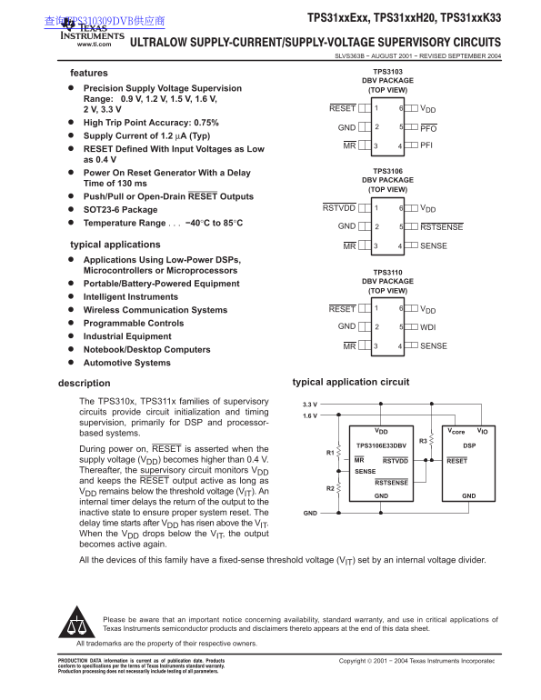
features TPS3103 DBV PACKAGE

Precision Supply Voltage Supervision (TOP VIEW) Range: 0.9 V, 1.2 V, 1.5 V, 1.6 V,

2 V, 3.3 V RESET VDD

High Trip Point Accuracy: 0.75%

GND PFO

Supply Current of 1.2 µA (Typ)

MR PFI

RESET Defined With Input Voltages as Low as 0.4 V

Power On Reset Generator With a Delay TPS3106 DBV PACKAGE

Time of 130 ms

(TOP VIEW)

Push/Pull or Open-Drain RESET Outputs

RSTVDD VDD

SOT23-6 Package Temperature Range −40°C to 85°C

GND RSTSENSE

typical applications MR SENSE Applications Using Low-Power DSPs, Microcontrollers or Microprocessors TPS3110

DBV PACKAGE

Portable/Battery-Powered Equipment

(TOP VIEW)

Intelligent Instruments

Wireless Communication Systems RESET VDD

Programmable Controls

GND WDI

Industrial Equipment

MR SENSE

Notebook/Desktop Computers Automotive Systems

description typical application circuit

The TPS310x, TPS311x families of supervisory

circuits provide circuit initialization and timing

supervision, primarily for DSP and processor-

VDD Vcore VIO

based systems.

TPS3106E33DBV DSP

During power on, RESET is asserted when the

supply voltage (VDD) becomes higher than 0.4 V. MR RSTVDD RESET

Thereafter, the supervisory circuit monitors VDD SENSE and keeps the RESET output active as long as RSTSENSE

VDD remains below the threshold voltage (VIT). An

GND GND

internal timer delays the return of the output to the inactive state to ensure proper system reset. The GND delay time starts after VDD has risen above the VIT. When the VDD drops below the VIT, the output becomes active again. All the devices of this family have a fixed-sense threshold voltage (VIT) set by an internal voltage divider.

Please be aware that an important notice concerning availability, standard warranty, and use in critical applications of Texas Instruments semiconductor products and disclaimers thereto appears at the end of this data sheet.

All trademarks are the property of their respective owners.

Page Summary Contents For Texas Instruments TPS31XXEXX Data Sheet

Page 1 查询TPS310309DVB供应商 www.ti.com SLVS363B − AUGUST 2001 − REVISED SEPTEMBER 2004 features TPS3103 DBV PACKAGE Precision Supply Voltage Supervision (TOP VIEW) Range: 0.9 V, 1.2 V, 1.5 V, 1.6 V, 2 V, 3.3 V ...
Page 2 www.ti.com SLVS363B − AUGUST 2001 − REVISED SEPTEMBER 2004 description (continued) The TPS3103 and TPS3106 have an active-low, open drain RESET output. The TPS3110 has an active-low push/pull RESET. T...
Page 3 www.ti.com SLVS363B − AUGUST 2001 − REVISED SEPTEMBER 2004 ordering information TPS31 DBV Reel Package Nominal Supply Voltage Typical Reset Threshold Voltage Functionality Family TYPICAL RESET NOMINAL...
Page 4 www.ti.com SLVS363B − AUGUST 2001 − REVISED SEPTEMBER 2004 functional block diagram TPS3103 RESET Reset Logic and Timer TPS3106 VDD VIT− RSTVDD Reset Logic and Timer RSTSENSE Reset Logic and Timer SEN...
Page 5 www.ti.com SLVS363B − AUGUST 2001 − REVISED SEPTEMBER 2004 functional block diagram (continued) TPS3110 VDD VIT− RESET Reset Logic SENSE and Timer Watchdog WDI Logic and Control
Page 6 www.ti.com SLVS363B − AUGUST 2001 − REVISED SEPTEMBER 2004 timing diagram SENSE VIT−(S) = 0.551 V td td td td RESET Output Condition Undefined Output Condition Undefined VIT−(S) = 0.551 V Output Condi...
Page 7 www.ti.com SLVS363B − AUGUST 2001 − REVISED SEPTEMBER 2004 timing diagram VDD VIT RSTVDD Output Condition Undefined Output Condition Undefined SENSE VIT−(S) = 0.551 V RSTSENSE Output Condition Undefin...
Page 8 www.ti.com SLVS363B − AUGUST 2001 − REVISED SEPTEMBER 2004 timing diagram VDD VIT SENSE VIT−(S) = 0.551 V td td td RESET td td Output Condition Undefined Output Condition Undefined t(tout) x = Don’t C...
Page 9 www.ti.com SLVS363B − AUGUST 2001 − REVISED SEPTEMBER 2004 Terminal Functions TERMINAL I/O DESCRIPTION NAME PART NO. GND ALL GND MR ALL Manual-reset input. Pull low to force a reset. RESET remains low...
Page 10 www.ti.com SLVS363B − AUGUST 2001 − REVISED SEPTEMBER 2004 SENSE The voltage at the SENSE input is compared with a reference voltage of 0.551 V. If the voltage at SENSE falls below the sense-threshold...
Page 11 www.ti.com SLVS363B − AUGUST 2001 − REVISED SEPTEMBER 2004 electrical characteristics over recommended operating conditions (unless otherwise noted) PARAMETERS TEST CONDITIONS MIN TYP MAX UNIT VDD = 3...
Page 12 www.ti.com SLVS363B − AUGUST 2001 − REVISED SEPTEMBER 2004 TIMING REQUIREMENTS AT RL = 1 MΩ, CL = 50 PF, TA = −40°C TO 85°C PARAMETER TEST CONDITIONS MIN TYP MAX UNIT tt(out) Time-out period at WDI VD...
Page 13 www.ti.com SLVS363B − AUGUST 2001 − REVISED SEPTEMBER 2004 ly rr en TYPICAL CHARACTERISTICS Table of Graphs FIGURE Supply current vs Supply voltage at TA = −40°C, 0°C, 25°C, 85°C VOL Low-level output ...
Page 14 ig -L ev el tp Vo lt ag www.ti.com -L ev el tp Vo lt ag SLVS363B − AUGUST 2001 − REVISED SEPTEMBER 2004 TPS3110E09 TPS3110E09 LOW-LEVEL OUTPUT VOLTAGE HIGH-LEVEL OUTPUT VOLTAGE vs vs LOW-LEVEL OUTPUT ...
Page 15 www.ti.com SLVS363B − AUGUST 2001 − REVISED SEPTEMBER 2004 NORMALIZED THRESHOLD VOLTAGE FREE-AIR TEMPERATURE rm al iz ed re sh ld lt ag 1.002 IT TA − Free-Air Temperature − °C Figure 10 APPLICATION IN...
Page 16 www.ti.com SLVS363B − AUGUST 2001 − REVISED SEPTEMBER 2004 APPLICATION INFORMATION VDD VDD MSP430 TPS3103H20 R1 Low Power µC MR Px.x Analog RESET RESET Circuit PFO Py.x GND GND R2 VDD V(neg_th) 0.551 ...
Page 17 www.ti.com SLVS363B − AUGUST 2001 − REVISED SEPTEMBER 2004 APPLICATION INFORMATION The TPS310x family has a quiescent current in the 1-µA to 2-µA range. When RESET, triggered by the voltage monitored ...
Page 18 PACKAGE OPTION ADDENDUM www.ti.com 8-Aug-2005 PACKAGING INFORMATION Orderable Device Status Package Package Pins Package Eco Plan Lead/Ball Finish MSL Peak Temp Type Drawing Qty TPS3103E12DBVR ACTIVE ...
Page 19 PACKAGE OPTION ADDENDUM www.ti.com 8-Aug-2005 Orderable Device Status Package Package Pins Package Eco Plan Lead/Ball Finish MSL Peak Temp Type Drawing Qty TPS3106K33DBVT ACTIVE SOT-23 DBV Green (Ro H...
Page 20 PACKAGE OPTION ADDENDUM www.ti.com 8-Aug-2005 Important Information and Disclaimer:The information provided on this page represents TI's knowledge and belief as of the date that it is provided. TI bas...
Page 22 IMPORTANT NOTICE Texas Instruments Incorporated and its subsidiaries (TI) reserve the right to make corrections, modifications, enhancements, improvements, and other changes to its products and servic...

Manual Details

Brand Texas Instruments
Pages 22
File Size 350.42 KB
Published June 17, 2026
2 views

Enter the captcha to get the download link:

captcha

Frequently Asked Questions

What is the primary function of the TPS310x/TPS311x family?

They provide circuit initialization and voltage supervision, primarily for DSP and processor core IO based systems.

How does the TPS3106 operate during power-on reset?

RESET is asserted when the supply voltage (V) rises above 0.4 V, and an internal timer delays output deactivation.

What temperature range can these supervisory circuits handle?

The TPS31xx family is characterized for operation over a temperature range of −40°C to 85°C.

Which model has an active-low push/pull RESET output?

The TPS3110 model utilizes an active-low push/pull RESET, while the TPS3103 and TPS3106 are open drain.