Texas Instruments TMS27C040 524288 by 8-bit UV erasable TMS27PC040 524288 by 8-bit programmable read-only memory Data Manual (1) User Guide
Summary
Discover high-capacity 8-bit electrically programmable memory solutions, including UV erasable EPROMs and one-time programmable (OTP) PROMs. These reliable read-only memories are essential components for microprocessor-based systems, offering robust performance in a single 5V supply environment while maintaining TTL compatibility across all inputs and outputs. This documentation provides detailed technical specifications covering various operation modes (read, program, standby), pin configurations, power requirements, and electrical guidelines necessary for seamless integration into your next electronic design. Ideal for hardware engineers designing complex digital circuits.
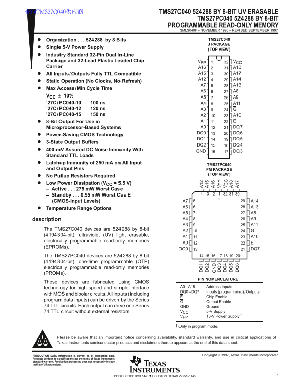
Page 1 Text Content
查询TMS27C040供应商 TMS27C040 524288 BY 8-BIT UV ERASABLE
TMS27PC040 524288 BY 8-BIT
PROGRAMMABLE READ-ONLY MEMORY SMLS040F – NOVEMBER 1990 – REVISED SEPTEMBER 1997
Organization 524288 by 8 Bits TMS27C040 J PACKAGE
Single 5-V Power Supply
(TOP VIEW)
Industry Standard 32-Pin Dual In-Line Package and 32-Lead Plastic Leaded Chip VPP VCC Carrier A16 A18
All Inputs/Outputs Fully TTL Compatible A15 A17 A12 A14
Static Operation (No Clocks, No Refresh)
Max Access/Min Cycle Time
VCC 10%
’27C/PC040-10 100 ns A4 A11 ’27C/PC040-12 120 ns A3 ’27C/PC040-15 150 ns A2 A10
8-Bit Output For Use in A1 Microprocessor-Based Systems A0 DQ7 DQ0 DQ6
Power-Saving CMOS Technology
DQ1 DQ5
3-State Output Buffers
DQ2 DQ4
400-m V Assured DC Noise Immunity With
GND DQ3
Standard TTL Loads Latchup Immunity of 250 m A on All Input
TMS27PC040
and Output Pins FM PACKAGE
(TOP VIEW)
No Pullup Resistors Required Low Power Dissipation (VCC = 5.5 V) – Active 275 m W Worst Case – Standby 0.55 m W Worst Cas E
(CMOS-Input Levels) A7 A14
Temperature Range Options
A5 A8 description A4 A9 A3 A11
The TMS27C040 devices are 524288 by 8-bit
(4194304-bit), ultraviolet (UV) light erasable,
electrically programmable read-only memories
(EPROMs).
DQ0 DQ7
The TMS27PC040 devices are 524288 by 8-bit (4194304-bit), one-time programmable (OTP) electrically programmable read-only memories (PROMs).
PIN NOMENCLATURE
These devices are fabricated using CMOS
A0–A18 Address Inputs
technology for high speed and simple interface
DQ0–DQ7 Inputs (programming) /Outputs
with MOS and bipolar circuits. All inputs ( including
Chip Enable
program data inputs) can be driven by the Series
Output Enable
74 TTL circuits. Each output can drive one Series GND Ground
74 TTL circuit without external resistors. VCC 5-V Supply VPP 13-V Power Supply†
Only in program mode.
Please be aware that an important notice concerning availability, standard warranty, and use in critical applications of Texas Instruments semiconductor products and disclaimers thereto appears at the end of this data sheet.
Copyright 1997, Texas Instruments Incorporated PRODUCTION DATA information is current as of publication date.
Products conform to specifications per the terms of Texas Instruments standard warranty. Production processing does not necessarily include testing of all parameters.
1POST OFFICE BOX 1443 • HOUSTON, TEXAS 77251–1443
Page Summary Contents For Texas Instruments TMS27C040 524288 by 8-bit UV erasable TMS27PC040 524288 by 8-bit programmable read-only memory Data Manual (1) User Guide
Manual Details
| Brand | Texas Instruments |
|---|---|
| Pages | 12 |
| File Size | 164.22 KB |
| Published | June 06, 2026 |
Enter the captcha to get the download link:

Frequently Asked Questions
How should I connect multiple devices of this type to a single bus?
The data outputs are designed as 3-state lines, which allows connection in parallel on the same bus without interference from competing outputs.
What different voltage levels are required for operation and programming?
A single 5-V supply is sufficient for read mode operation, but an additional 13 V supply is needed specifically for the programming function.
Do I need external resistors when connecting this device to a system bus?
No; all outputs can drive one series GND or V 5-V TTL circuit without requiring external resistors.
What thermal range choices are available for selecting the correct module?
Modules are offered with two temperature ranges: 0°C to 70°C (JL suffix) or –40°C to 85°C (JE suffix).