# A B C D E F G H I J K L M N O P Q R S T U V W X Y Z

Texas Instruments TLV2606 Data Sheet

Summary

The TLV5606 is a high-performance 10-bit voltage output Digital-to-Analog Converter (DAC) engineered for precision control applications. Featuring a flexible 4-wire serial interface, it allows stable measurement and signal generation across industrial and motion control systems. The manual details its customizable features, including programmable settling time to optimize speed versus power use, differential linearity specifications, और rail-to-rail output buffering. Ideal for engineers designing robust solutions in process control, data acquisition, and embedded systems requiring reliable, low-power voltage reference signals.
📄 Preview 📖 Table of Contents Contents PAGE OF 22

Page 1 Text Content

SLAS259B − DECEMBER 1999 − REVISED APRIL 2004

features Buffered High-Impedance Reference Input Voltage Output Range . 2 Times the

10-Bit Voltage Output DAC

Reference Input Voltage

Programmable Settling Time vs Power

Monotonic Over Temperature

Consumption 3 µs in Fast Mode Available in MSOP Package 9 µs in Slow Mode

Ultra Low Power Consumption: applications

900 µW Typ in Slow Mode at 3 V

Digital Servo Control Loops

2.1 m W Typ in Fast Mode at 3 V

Digital Offset and Gain Adjustment

Differential Nonlinearity <0.2 LSB Typ

Industrial Process Control

Compatible With TMS320 and SPI Serial

Machine and Motion Control Devices

Ports

Mass Storage Devices

Power-Down Mode (10 n A)

D OR DGK PACKAGE

description

(TOP VIEW)

The TLV5606 is a 10-bit voltage output digital-to-

analog converter (DAC) with a flexible 4-wire DIN VDD

serial interface. The 4-wire serial interface allows SCLK OUT glueless interface to TMS320, SPI, QSPI, and CS REFIN

Microwire serial ports. The TLV5606 is pro- FS AGND

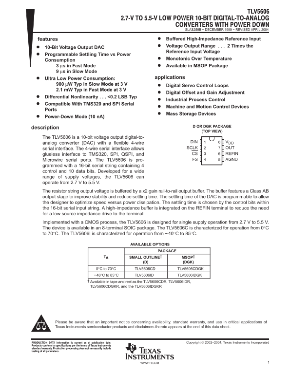
grammed with a 16-bit serial string containing 4 control and 10 data bits. Developed for a wide range of supply voltages, the TLV5606 can operate from 2.7 V to 5.5 V. The resistor string output voltage is buffered by a x2 gain rail-to-rail output buffer. The buffer features a Class AB output stage to improve stability and reduce settling time. The settling time of the DAC is programmable to allow the designer to optimize speed versus power dissipation. The settling time is chosen by the control bits within the 16-bit serial input string. A high-impedance buffer is integrated on the REFIN terminal to reduce the need for a low source impedance drive to the terminal. Implemented with a CMOS process, the TLV5606 is designed for single supply operation from 2.7 V to 5.5 V. The device is available in an 8-terminal SOIC package. The TLV5606C is characterized for operation from 0°C to 70°C. The TLV5606I is characterized for operation from −40°C to 85°C.

AVAILABLE OPTIONS

PACKAGE

TA SMALL OUTLINE† MSOP†

(D) (DGK)

0°C to 70°C TLV5606CD TLV5606CDGK −40°C to 85°C TLV5606ID TLV5606IDGK Available in tape and reel as the TLV5606CDR, TLV5606IDR, TLV5606CDGKR, and the TLV5606IDGKR

Please be aware that an important notice concerning availability, standard warranty, and use in critical applications of Texas Instruments semiconductor products and disclaimers thereto appears at the end of this data sheet.

1WWW.TI.COM

Page Summary Contents For Texas Instruments TLV2606 Data Sheet

Page 1 SLAS259B − DECEMBER 1999 − REVISED APRIL 2004 features Buffered High-Impedance Reference Input Voltage Output Range . 2 Times the 10-Bit Voltage Output DAC Reference Input Voltage Programmable Settlin...
Page 2 SLAS259B − DECEMBER 1999 − REVISED APRIL 2004 functional block diagram REFIN Serial Input DIN 10-Bit Register x2 OUT Latch 16 Cycle Update Timer Power-On Reset Speed/Power-Down Logic Terminal Function...
Page 3 SLAS259B − DECEMBER 1999 − REVISED APRIL 2004 absolute maximum ratings over operating free-air temperature range (unless otherwise noted)† Supply voltage (VDD to AGND) 7 V. . . . . . . . . . . . . . ....
Page 4 SLAS259B − DECEMBER 1999 − REVISED APRIL 2004 electrical characteristics over recommended operating free-air temperature range (unless otherwise noted) (continued) static DAC specifications RL = 10 kΩ...
Page 5 SLAS259B − DECEMBER 1999 − REVISED APRIL 2004 operating characteristics over recommended operating free-air temperature range (unless otherwise noted) analog output dynamic performance PARAMETER TEST ...
Page 6 SLAS259B − DECEMBER 1999 − REVISED APRIL 2004 PARAMETER MEASUREMENT INFORMATION tw Htw L SCLK ÎÎÎÎÎ ÎÎÎ th(D)tsu(D) DIN ÎÎÎÎ D15 D14 D13 D12 D1 D0 ÎÎÎÎ tsu(FS-CK) tsu(C16-CS) tsu(CS-FS) tw H(FS) tsu(C...
Page 7 SLAS259B − DECEMBER 1999 − REVISED APRIL 2004 tp Vo lt ag tp Vo lt ag TYPICAL CHARACTERISTICS OUTPUT VOLTAGE OUTPUT VOLTAGE vs vs LOAD CURRENT LOAD CURRENT 3 V Slow Mode, SOURCE VDD = 3 V, VDD = 5 V, ...
Page 8 ly rr en ta l H ar ic is to rt io SLAS259B − DECEMBER 1999 − REVISED APRIL 2004 TYPICAL CHARACTERISTICS SUPPLY CURRENT SUPPLY CURRENT vs vs FREE-AIR TEMPERATURE FREE-AIR TEMPERATURE VDD = 3 V, VDD = 5...
Page 9 SLAS259B − DECEMBER 1999 − REVISED APRIL 2004 ta l H ar ic is to rt io is TYPICAL CHARACTERISTICS TOTAL HARMONIC DISTORTION AND NOISE TOTAL HARMONIC DISTORTION AND NOISE vs vs FREQUENCY FREQUENCY Vref...
Page 10 SLAS259B − DECEMBER 1999 − REVISED APRIL 2004 TYPICAL CHARACTERISTICS if fe re ti al lin ea ri ty IN In te ra l N lin ea ri ty INTEGRAL NONLINEARITY ERROR Digital Code Figure 13 DIFFERENTIAL NONLINEAR...
Page 11 SLAS259B − DECEMBER 1999 − REVISED APRIL 2004 APPLICATION INFORMATION general function The TLV5606 is a 10-bit single supply DAC based on a resistor string architecture. The device consists of a seria...
Page 12 SLAS259B − DECEMBER 1999 − REVISED APRIL 2004 APPLICATION INFORMATION serial interface (continued) If there is no need to have more than one device on the serial bus, then CS can be tied low. Figure 1...
Page 13 SLAS259B − DECEMBER 1999 − REVISED APRIL 2004 APPLICATION INFORMATION TLV5606 interfaced to TMS320C203 DSP hardware interfacing Figure 17 shows an example how to connect the TLV5606 to a TMS320C203 DS...
Page 14 SLAS259B − DECEMBER 1999 − REVISED APRIL 2004 APPLICATION INFORMATION ;* Main Program .ps 1000h .entry start: ; disable interrupts setc INTM ; disable maskable interrupts splk #0ffffh, IFR splk #0004h...
Page 15 SLAS259B − DECEMBER 1999 − REVISED APRIL 2004 APPLICATION INFORMATION TLV5606 interfaced to MCS51 microcontroller hardware interfacing Figure 18 shows an example of how to connect the TLV5606 to an M...
Page 16 SLAS259B − DECEMBER 1999 − REVISED APRIL 2004 APPLICATION INFORMATION LJMP start ; Execution starts at address 0 on power−up. ;−−−−−−−−−−−−−−−−−−−−−−−−−−−−−−−−−−−−−−−−−−−−−−−−−−−−−−−−−−−−−−−−−−−−−−−−−...
Page 17 SLAS259B − DECEMBER 1999 − REVISED APRIL 2004 APPLICATION INFORMATION RSEG STACK DS 10h ; 16 Byte Stack! ;−−−−−−−−−−−−−−−−−−−−−−−−−−−−−−−−−−−−−−−−−−−−−−−−−−−−−−−−−−−−−−−−−−−−−−−−−−−−−−− ; Main Program...
Page 18 SLAS259B − DECEMBER 1999 − REVISED APRIL 2004 APPLICATION INFORMATION linearity, offset, and gain error using single ended supplies When an amplifier is operated from a single supply, the voltage offs...
Page 19 SLAS259B − DECEMBER 1999 − REVISED APRIL 2004 APPLICATION INFORMATION definitions of specifications and terminology integral nonlinearity (INL) The relative accuracy or integral nonlinearity (INL), so...
Page 22 IMPORTANT NOTICE Texas Instruments Incorporated and its subsidiaries (TI) reserve the right to make corrections, modifications, enhancements, improvements, and other changes to its products and servic...

Manual Details

Brand Texas Instruments
Pages 22
File Size 434.85 KB
Published June 18, 2026
2 views

Enter the captcha to get the download link:

captcha

Frequently Asked Questions

What is the operating voltage range for this DAC?

The TLV5606 can operate from a wide supply voltage range of 2.7 V to 5.5 V.

How is the settling time configured on this device?

The settling time is programmable and can be optimized by selecting control bits within the 16-bit serial input string, balancing speed versus power dissipation.

In what environments can the TLV5606 function?

It is available in two versions: TLV5606C for 0°C to 70°C (<span style='font-style:italic'>Operating free-air temperature</span>) and TLV5606I for -40°C to 85°C.

What is the power consumption in different operating modes?

The average current consumption varies by mode; for example, it is 900 µW Typ in Slow Mode at 3 V, and Digital Servo Control Loops consume about 2.1 mW Typ in Fast Mode at 3 V.