Texas Instruments - TLC551, TLC551Y Data Sheet
Summary
The TLC551 is a highly accurate monolithic timing circuit designed for reliable oscillation and time delay applications. This low-power IC offers superior performance over traditional timers while maintaining compatibility with CMOS, TTL, and MOS logic. The accompanying manual provides comprehensive technical details on its operation, covering functional modes, reset priority inputs, high ESD protection (up to 2kV), and optimal design guidelines. It is essential documentation for electronics engineers seeking a stable, precise timing solution in complex digital circuits.
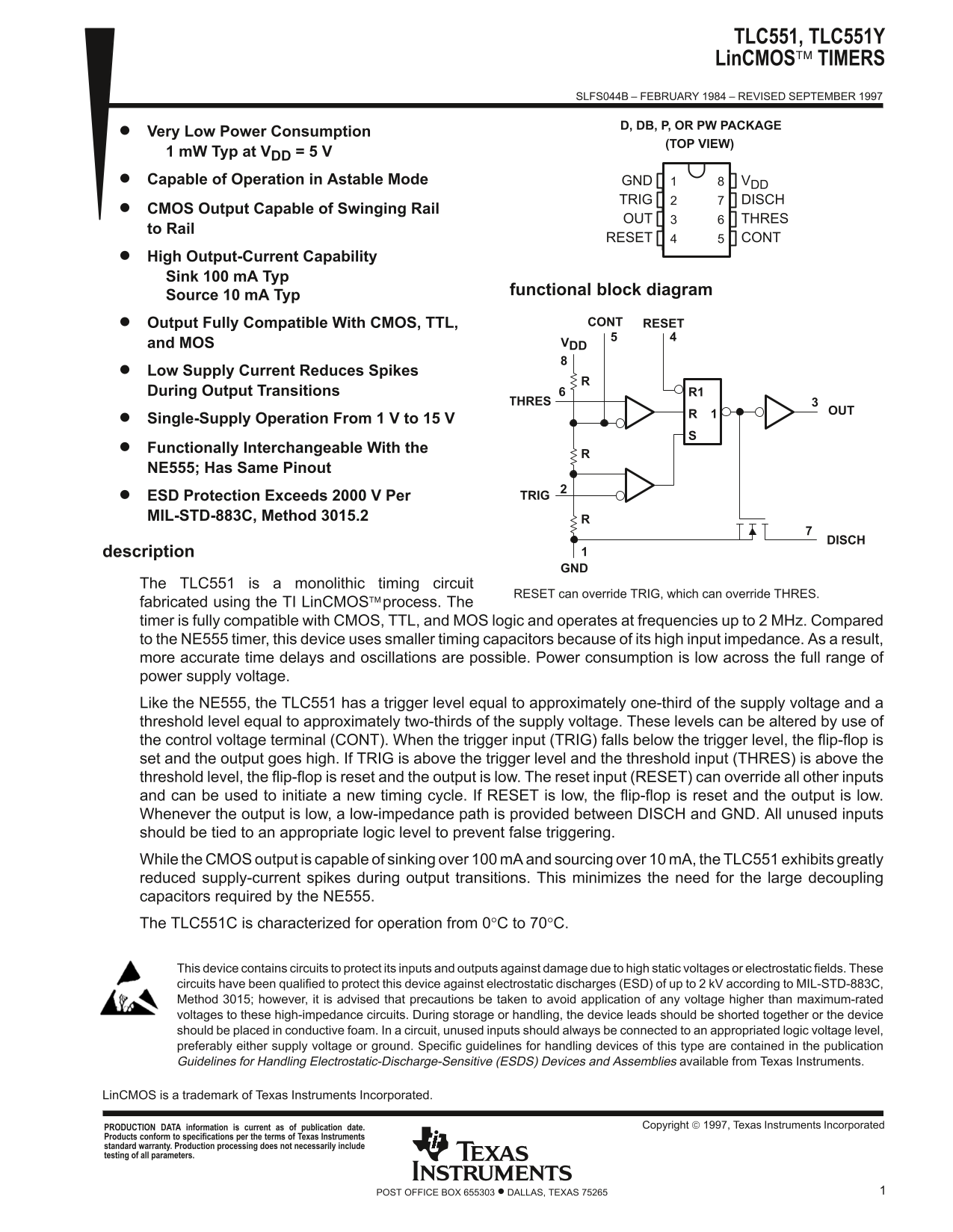
Page 1 Text Content
TLC551, TLC551Y Lin CMOS TIMERS
SLFS044B – FEBRUARY 1984 – REVISED SEPTEMBER 1997
D, DB, P, OR PW PACKAGE
Very Low Power Consumption
(TOP VIEW)
1 m W Typ at VDD = 5 V Capable of Operation in Astable Mode GND VDD
TRIG DISCH
CMOS Output Capable of Swinging Rail
OUT THRES
to Rail
RESET CONT
High Output-Current Capability Sink 100 m A Typ
functional block diagram
Source 10 m A Typ
Output Fully Compatible With CMOS, TTL, RESETCONT
and MOS VDD
Low Supply Current Reduces Spikes During Output Transitions R1
THRES
Single-Supply Operation From 1 V to 15 V Functionally Interchangeable With the NE555; Has Same Pinout
ESD Protection Exceeds 2000 V Per TRIG
MIL-STD-883C, Method 3015.2
DISCH
description
The TLC551 is a monolithic timing circuit
RESET can override TRIG, which can override THRES.
fabricated using the TI Lin CMOSprocess. The timer is fully compatible with CMOS, TTL, and MOS logic and operates at frequencies up to 2 MHz. Compared to the NE555 timer, this device uses smaller timing capacitors because of its high input impedance. As a result, more accurate time delays and oscillations are possible. Power consumption is low across the full range of power supply voltage. Like the NE555, the TLC551 has a trigger level equal to approximately one-third of the supply voltage and a threshold level equal to approximately two-thirds of the supply voltage. These levels can be altered by use of the control voltage terminal (CONT). When the trigger input (TRIG) falls below the trigger level, the flip-flop is set and the output goes high. If TRIG is above the trigger level and the threshold input (THRES) is above the threshold level, the flip-flop is reset and the output is low. The reset input (RESET) can override all other inputs and can be used to initiate a new timing cycle. If RESET is low, the flip-flop is reset and the output is low. Whenever the output is low, a low-impedance path is provided between DISCH and GND. All unused inputs should be tied to an appropriate logic level to prevent false triggering. While the CMOS output is capable of sinking over 100 m A and sourcing over 10 m A, the TLC551 exhibits greatly reduced supply-current spikes during output transitions. This minimizes the need for the large decoupling capacitors required by the NE555. The TLC551C is characterized for operation from 0°C to 70°C.
This device contains circuits to protect its inputs and outputs against damage due to high static voltages or electrostatic fields. These circuits have been qualified to protect this device against electrostatic discharges (ESD) of up to 2 k V according to MIL-STD-883C, Method 3015; however, it is advised that precautions be taken to avoid application of any voltage higher than maximum-rated voltages to these high-impedance circuits. During storage or handling, the device leads should be shorted together or the device should be placed in conductive foam. In a circuit, unused inputs should always be connected to an appropriated logic voltage level, preferably either supply voltage or ground. Specific guidelines for handling devices of this type are contained in the publication Guidelines for Handling Electrostatic-Discharge-Sensitive (ESDS) Devices and Assemblies available from Texas Instruments.
Lin CMOS is a trademark of Texas Instruments Incorporated.
Copyright 1997, Texas Instruments Incorporated PRODUCTION DATA information is current as of publication date.
Products conform to specifications per the terms of Texas Instruments standard warranty. Production processing does not necessarily include testing of all parameters.
1POST OFFICE BOX 655303 • DALLAS, TEXAS 75265
Page Summary Contents For Texas Instruments - TLC551, TLC551Y Data Sheet
Manual Details
| Brand | Texas Instruments |
|---|---|
| Pages | 16 |
| File Size | 276.28 KB |
| Published | July 15, 2026 |
Enter the captcha to get the download link:

Frequently Asked Questions
What power supplies can the TLC551 operate from?
It supports single-supply operation ranging from 1 V to 15 V, and maximum voltage options exist up to 16V.
What must I do with unused inputs to prevent false triggering?
Unused inputs should always be connected to an appropriate logic level, preferably either supply voltage or ground.
How does the TLC551 match or improve upon the NE555 timer?
It is functionally interchangeable, but uses high input impedance and has a reduced supply-current spike, allowing for more accurate time delays.
What is the recommended procedure when handling this circuit board?
During storage or handling, the device leads should be shorted together or placed in conductive foam due to its high ESD protection.