Texas Instruments TLC27M2, TLC27M2A, TLC27M2B, TLC27M7 LinCMOS PRECISION DUAL OPERATIONAL AMPLIFIERS Data Sheet User Manual
Summary
Boost your analog designs with the TLC27M dual operational amplifiers. These high-precision ICs utilize robust LinCMOS technology to provide exceptionally low noise, minimal offset voltage drift, and reliable single-supply operation compatible with negative rails. The corresponding documentation provides comprehensive details on various grades (TLC27M2/M7), full temperature ranges (-55°C to 125°C), packaging options, and advanced electrical specifications. Essential for engineers designing state-of-the-art analog circuits, active filters, signal buffers, or portable battery-powered systems requiring high stability.
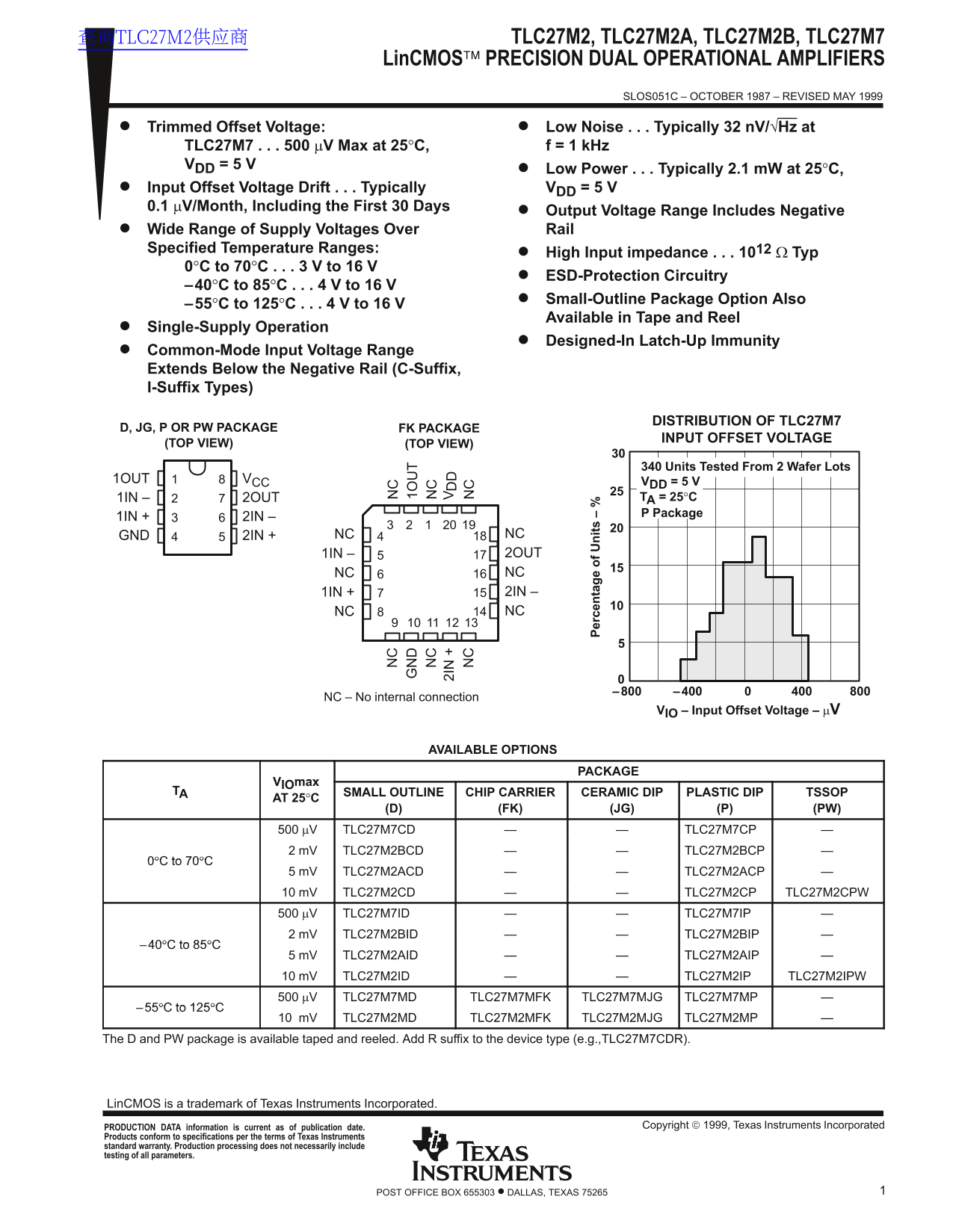
Page 1 Text Content
查询TLC27M2供应商 TLC27M2, TLC27M2A, TLC27M2B, TLC27M7
Lin CMOS PRECISION DUAL OPERATIONAL AMPLIFIERS
SLOS051C – OCTOBER 1987 – REVISED MAY 1999
Trimmed Offset Voltage: Low Noise Typically 32 n V/√Hz at TLC27M7 500 µV Max at 25°C, f = 1 k Hz VDD = 5 V
Low Power Typically 2.1 m W at 25°C, Input Offset Voltage Drift Typically VDD = 5 V
0.1 µV/Month, Including the First 30 Days
Output Voltage Range Includes Negative Wide Range of Supply Voltages Over Rail
Specified Temperature Ranges:
High Input impedance 1012 Ω Typ
0°C to 70°C 3 V to 16 V
ESD-Protection Circuitry
–40°C to 85°C 4 V to 16 V
Small-Outline Package Option Also
–55°C to 125°C 4 V to 16 V
Available in Tape and Reel
Single-Supply Operation
Designed-In Latch-Up Immunity
Common-Mode Input Voltage Range Extends Below the Negative Rail (C-Suffix, I-Suffix Types)
DISTRIBUTION OF TLC27M7
D, JG, P OR PW PACKAGE FK PACKAGE
INPUT OFFSET VOLTAGE
(TOP VIEW) (TOP VIEW)
ÎÎÎÎÎÎÎÎÎÎÎ340 Units Tested From 2 Wafer Lots
1OUT VCC VDD = 5 V
1IN 2OUT TA = 25°C P Package
1IN 2IN
GND 2IN NC NC 1IN 2OUT NC NC 1IN 2IN
er ce ta it
NC NC
NC – No internal connection
VIO – Input Offset Voltage – µV
AVAILABLE OPTIONS
PACKAGE
VIOmax
TA SMALL OUTLINE CHIP CARRIER CERAMIC DIP PLASTIC DIP TSSOP
AT 25°C
(D) (FK) (JG) (P) (PW)
500 µV TLC27M7CD TLC27M7CP 2 m V TLC27M2BCD TLC27M2BCP
0°C to 70°C
5 m V TLC27M2ACD TLC27M2ACP 10 m V TLC27M2CD TLC27M2CP TLC27M2CPW 500 µV TLC27M7ID TLC27M7IP 2 m V TLC27M2BID TLC27M2BIP
40°C to 85°C
5 m V TLC27M2AID TLC27M2AIP 10 m V TLC27M2ID TLC27M2IP TLC27M2IPW 500 µV TLC27M7MD TLC27M7MFK TLC27M7MJG TLC27M7MP
55°C to 125°C
10 m V TLC27M2MD TLC27M2MFK TLC27M2MJG TLC27M2MP
The D and PW package is available taped and reeled. Add R suffix to the device type (e.g.,TLC27M7CDR).
Lin CMOS is a trademark of Texas Instruments Incorporated.
Copyright 1999, Texas Instruments Incorporated PRODUCTION DATA information is current as of publication date.
Products conform to specifications per the terms of Texas Instruments standard warranty. Production processing does not necessarily include testing of all parameters.
1POST OFFICE BOX 655303 • DALLAS, TEXAS 75265
Page Summary Contents For Texas Instruments TLC27M2, TLC27M2A, TLC27M2B, TLC27M7 LinCMOS PRECISION DUAL OPERATIONAL AMPLIFIERS Data Sheet User Manual
Manual Details
| Brand | Texas Instruments |
|---|---|
| Pages | 34 |
| File Size | 511.51 KB |
| Published | July 15, 2026 |
Enter the captcha to get the download link:

Frequently Asked Questions
What operating temperature range is suitable for the M-suffix devices?
The M-suffix devices are characterized for operation over the full military temperature range of –55°C to 125°C.
How does the device handle common-mode inputs?
The common-mode input voltage range includes the negative rail, and the common-mode rejection is good.
Which models are best for high precision applications?
The TLC27M7 offers the highest precision, with an available 500 μV offset voltage grade.
Are these amplifiers suitable for battery-powered use?
Yes, they exhibit low voltage single-supply operation, making them ideally suited for remote and inaccessible battery-powered applications.