Texas Instruments THS0842 Data Sheet
Summary
The Texas Instruments THS0842 is a dual-input 8-bit 40 MSPS analog-to-digital converter designed for high-speed signal acquisition. It features dual simultaneous sample-and-hold inputs, differential or single-ended analog inputs, 600 MHz analog input bandwidth, 3.3V single-supply operation, and 275mW low power consumption. Applications include digital communications, cable modems, set-top boxes, and test instruments. Target users are RF and mixed-signal design engineers developing high-speed data acquisition systems.
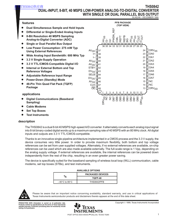
Page 1 Text Content
查询THS0842供应商 THS0842
DUAL-INPUT, 8-BIT, 40 MSPS LOW-POWER ANALOG-TO-DIGITAL CONVERTER
WITH SINGLE OR DUAL PARALLEL BUS OUTPUT
SLAS246 – DECEMBER 1999
features PFB PACKAGE (TOP VIEW)
Dual Simultaneous Sample and Hold Inputs Differential or Single-Ended Analog Inputs 8-Bit Resolution 40 MSPS Sampling Analog-to-Digital Converter (ADC) Single or Dual Parallel Bus Output Low Power Consumption: 275 m W Typ
AVDD DRVSS
Using External References
I+ DA0
Wide Analog Input Bandwidth: 600 MHz Typ
I– DA1
3.3 V Single-Supply Operation
AVSS DA2
3.3 V TTL/CMOS-Compatible Digital I/O AVDD DA3
Internal or External Bottom and Top STBY DA4 Reference Voltages DVSS DA5 SELB DA6
Adjustable Reference Input Range
DVDD DA7
Power-Down (Standby) Mode
AVSS NC
48-Pin Thin Quad Flat Pack (TQFP)
CLK NC
Package
OE DRVDD
applications Digital Communications (Baseband Sampling) Cable Modems Set Top Boxes
Test Instruments
description The THS0842 is a dual 8-bit 40 MSPS high-speed A/D converter. It alternately converts each analog input signal into 8-bit binary-coded digital words up to a maximum sampling rate of 40 MSPS with an 80 MHz clock. All digital inputs and outputs are 3.3 V TTL/CMOS-compatible. Thanks to an innovative single-pipeline architecture implemented in a CMOS process and the 3.3 V supply, the
device consumes very little power. In order to provide maximum flexibility, both bottom and top voltage references can be set from user supplied voltages. Alternately, if no external references are available, on-chip references can be used which are also made available externally. The full-scale range is 1 Vpp, depending on the analog supply voltage. If external references are available, the internal references can be powered down independently from the rest of the chip, resulting in an even greater power saving. The device is specifically suited for the baseband sampling of wireless local loop (WLL) communication, cable modems, set top boxes (STBs), and test instruments.
AVAILABLE OPTIONS PACKAGED DEVICES
TQFP-48
–40°C to 85°C THS0842IPFB
Please be aware that an important notice concerning availability, standard warranty, and use in critical applications of Texas Instruments semiconductor products and disclaimers thereto appears at the end of this data sheet.
PRODUCTION DATA information is current as of publication date. Copyright 1999, Texas Instruments Incorporated
Products conform to specifications per the terms of Texas Instruments standard warranty. Production processing does not necessarily include testing of all parameters.
1POST OFFICE BOX 655303 • DALLAS, TEXAS 75265
Page Summary Contents For Texas Instruments THS0842 Data Sheet
Manual Details
| Brand | Texas Instruments |
|---|---|
| Pages | 29 |
| File Size | 478.75 KB |
| Published | June 16, 2026 |
Enter the captcha to get the download link:

Frequently Asked Questions
What is the operating temperature range for the THS0842?
The operating temperature range for the THS0842IPFB is -40°C to 85°C.
What are the typical applications for the THS0842?
Typical applications include digital communications, cable modems, set-top boxes, and test instruments.
What is the typical power consumption of the THS0842?
Typical power consumption is 275 mW when using external references.
What supply voltage does the THS0842 require?
It requires a single 3.3 V supply for operation and its digital I/O.