Texas Instruments SN74LVC3G07 Data Sheet
Summary
The SN74LVC3G07 is a high-performance triple buffer/driver designed for reliable digital interfacing in low-power systems (1.65V to 5.5V). Featuring open-drain outputs, it supports implementing active-low wired-OR or active-high wired-AND logic functions. This manual provides thorough technical documentation for hardware designers and engineers, covering electrical specifications, package options (including NanoStar™/NanoFree™), thermal data, and necessary guidelines for robust PCB design integration.
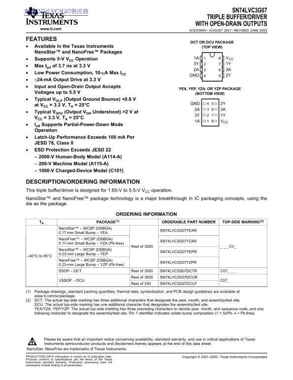
Page 1 Text Content
查询SN74LVC3G07供应商 SN74LVC3G07
TRIPLE BUFFER/DRIVER
WITH OPEN-DRAIN OUTPUTS
www.ti.com
SCES365H–AUGUST 2001–REVISED JUNE
FEATURES
DCT OR DCU PACKAGE
Available in the Texas Instruments (TOP VIEW)
Nano Star™ and Nano Free™ Packages
1A VCC
Supports 5-V VCC Operation
Max tpd of 3.7 ns at 3.3
Low Power Consumption, 10-µA Max ICC
GND 2Y
±24-m A Output Drive at 3.3
Input and Open-Drain Output Accepts
YEA, YEP, YZA, OR YZP PACKAGE
Voltages up to 5.5
(BOTTOM VIEW)
Typical VOLP (Output Ground Bounce) <0.8
GND 2Y
at VCC 3.3 V, TA 25°C
Typical VOHV (Output VOH Undershoot) >2 at
VCC 3.3 V, TA 25°C
1A VCC
Ioff Supports Partial-Power-Down Mode
Operation
Latch-Up Performance Exceeds m A Per
JESD 78, Class II
ESD Protection Exceeds JESD
2000-V Human-Body Model (A114-A)
200-V Machine Model (A115-A)
1000-V Charged-Device Model (C101)
DESCRIPTION/ORDERING INFORMATION
This triple buffer/driver is designed for 1.65-V to 5.5-V VCC operation.
Nano Star™ and Nano Free™ package technology is major breakthrough in IC packaging concepts, using the
die as the package.
ORDERING INFORMATION
TA PACKAGE ORDERABLE PART NUMBER TOP-SIDE MARKING
Nano Star™ WCSP (DSBGA)
SN74LVC3G07YEAR0.17-mm
Small Bump YEA
Nano Free™ WCSP (DSBGA)
SN74LVC3G07YZAR0.17-mm
Small Bump YZA (Pb-free)
Reel of _CV_
Nano Star™ WCSP (DSBGA)
SN74LVC3G07YEPR0.23-mm
Large Bump YEP–40°C
to 85°C
Nano Free™ WCSP (DSBGA)
SN74LVC3G07YZPR0.23-mm
Large Bump YZP (Pb-free)
SSOP DCT Reel of SN74LVC3G07DCTR C07_
Reel of SN74LVC3G07DCUR
VSSOP DCU C07_
Reel of SN74LVC3G07DCUT
(1) Package drawings, standard packing quantities, thermal data, symbolization, and PCB design guidelines are available at
www.ti.com/sc/package.
(2) DCT: The actual top-side marking has three additional characters that designate the year, month, and assembly/test site.
DCU: The actual top-side marking has one additional character that designates the assembly/test site.
YEA/YZA, YEP/YZP: The actual top-side marking has three preceding characters to denote year, month, and sequence code, and one
following character to designate the assembly/test site. Pin identifier indicates solder-bump composition (1 Sn Pb, Pb-free).
Please be aware that an important notice concerning availability, standard warranty, and use in critical applications of Texas
Instruments semiconductor products and disclaimers thereto appears at the end of this data sheet.
Nano Star, Nano Free are trademarks of Texas Instruments.
PRODUCTION DATA information is current as of publication date. Copyright 2001–2005, Texas Instruments Incorporated
Products conform to specifications per the terms of the Texas
Instruments standard warranty. Production processing does not
necessarily include testing of all parameters.
Page Summary Contents For Texas Instruments SN74LVC3G07 Data Sheet
Manual Details
| Brand | Texas Instruments |
|---|---|
| Pages | 13 |
| File Size | 325.82 KB |
| Published | June 02, 2026 |
Enter the captcha to get the download link:

Frequently Asked Questions
How can I connect multiple units using this buffer/driver?
The open-drain outputs allow connection to other open-drain outputs to implement active-low wired-OR or active-high wired-AND functions.
What is the primary operating voltage range for the device?
The SN74LVC3G07 is designed for operation within a wide range, supporting 1.65 V up to 5.5 V.
Does the chip support power saving or low-power modes?
Yes, it fully supports Partial-Power-Down mode. The dedicated circuitry disables outputs when powered down, preventing damaging current backflow.
Which packaging options are suitable for Pb-free requirements?
The orderable part numbers associated with the YZA or YZP identifiers correspond to lead-free (Pb-free) packages.