Texas Instruments SN74LVC2G66 Dual Bilateral Analog Switch Data Sheet
Summary
The SN74LVC2G66 is a versatile dual bilateral analog switch designed for reliable signal management in both analog and digital systems, operating across 1.65V to 5.5V. Ideal for engineers working on complex data conversion, signal gating, chopping circuits, or modem applications, this component features low on-state resistance and rail-to-rail I/O capability. This manual provides comprehensive technical details, including advanced packaging solutions (NanoStar™, NanoFree™), electrical specifications, and application guidelines necessary for professional circuit design and implementation.
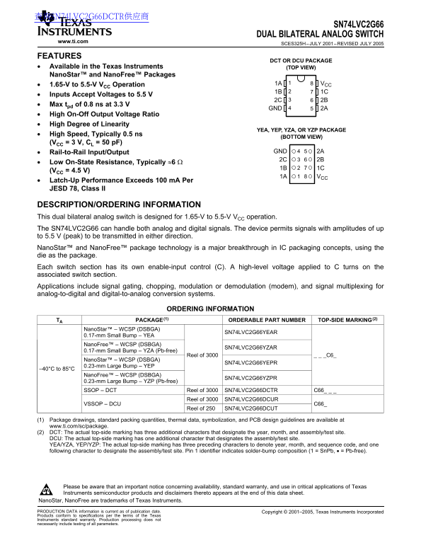
Page 1 Text Content
查询SN74LVC2G66DCTR供应商
SN74LVC2G66
DUAL BILATERAL ANALOG SWITCH
www.ti.com
SCES325H–JULY 2001–REVISED JULY
FEATURES
DCT OR DCU PACKAGE
Available in the Texas Instruments (TOP VIEW)
Nano Star™ and Nano Free™ Packages
1.65-V to 5.5-V VCC Operation 1A VCC
Inputs Accept Voltages to 5.5
Max tpd of 0.8 ns at 3.3
GND 2A
High On-Off Output Voltage Ratio
High Degree of Linearity
YEA, YEP, YZA, OR YZP PACKAGE
High Speed, Typically 0.5 ns
(BOTTOM VIEW)
(VCC V, CL p F)
Rail-to-Rail Input/Output GND 2A
Low On-State Resistance, Typically ≈6
(VCC 4.5 V)
1A VCC
Latch-Up Performance Exceeds m A Per
JESD 78, Class II
DESCRIPTION/ORDERING INFORMATION
This dual bilateral analog switch is designed for 1.65-V to 5.5-V VCC operation.
The SN74LVC2G66 can handle both analog and digital signals. The device permits signals with amplitudes of up
to 5.5 (peak) to be transmitted in either direction.
Nano Star™ and Nano Free™ package technology is major breakthrough in IC packaging concepts, using the
die as the package.
Each switch section has its own enable-input control (C). high-level voltage applied to turns on the
associated switch section.
Applications include signal gating, chopping, modulation or demodulation (modem), and signal multiplexing for
analog-to-digital and digital-to-analog conversion systems.
ORDERING INFORMATION
TA PACKAGE ORDERABLE PART NUMBER TOP-SIDE MARKING
Nano Star™ WCSP (DSBGA)
SN74LVC2G66YEAR0.17-mm
Small Bump YEA
Nano Free™ WCSP (DSBGA)
SN74LVC2G66YZAR0.17-mm
Small Bump YZA (Pb-free)
Reel of _C6_
Nano Star™ WCSP (DSBGA)
SN74LVC2G66YEPR0.23-mm
Large Bump YEP–40°C
to 85°C
Nano Free™ WCSP (DSBGA)
SN74LVC2G66YZPR0.23-mm
Large Bump YZP (Pb-free)
SSOP DCT Reel of SN74LVC2G66DCTR C66_
Reel of SN74LVC2G66DCUR
VSSOP DCU C66_
Reel of SN74LVC2G66DCUT
(1) Package drawings, standard packing quantities, thermal data, symbolization, and PCB design guidelines are available at
www.ti.com/sc/package.
(2) DCT: The actual top-side marking has three additional characters that designate the year, month, and assembly/test site.
DCU: The actual top-side marking has one additional character that designates the assembly/test site.
YEA/YZA, YEP/YZP: The actual top-side marking has three preceding characters to denote year, month, and sequence code, and one
following character to designate the assembly/test site. Pin identifier indicates solder-bump composition (1 Sn Pb, Pb-free).
Please be aware that an important notice concerning availability, standard warranty, and use in critical applications of Texas
Instruments semiconductor products and disclaimers thereto appears at the end of this data sheet.
Nano Star, Nano Free are trademarks of Texas Instruments.
PRODUCTION DATA information is current as of publication date. Copyright 2001–2005, Texas Instruments Incorporated
Products conform to specifications per the terms of the Texas
Instruments standard warranty. Production processing does not
necessarily include testing of all parameters.
Page Summary Contents For Texas Instruments SN74LVC2G66 Dual Bilateral Analog Switch Data Sheet
Manual Details
| Brand | Texas Instruments |
|---|---|
| Pages | 19 |
| File Size | 409.45 KB |
| Published | June 06, 2026 |
Enter the captcha to get the download link:

Frequently Asked Questions
What is the recommended operating voltage range?
The dual bilateral analog switch supports operation from 1.65 V to 5.5 V.
What types of signals can this device manage?
It is designed to handle both analog and digital signals with amplitudes up to 5.5 V (peak).
How are the individual switch sections activated or controlled?
Each switch section has its own enabling control input (C), which must be applied a high-level voltage to turn on.
What real-world applications can this component be used for?
Common applications include signal gating, chopping, modulation/demodulation, and signal multiplexing.