Texas Instruments SN74CBT3125C Data Sheet
Summary
A high-speed, TTL-compatible FET bus switch designed for reliable signal isolation and data transfer across various digital and analog interfaces. This device can function as four independent 1-bit switches or a single 4-bit bus switcher, featuring low ON-state resistance and active undershoot protection up to -2V. The manual provides comprehensive details on its functionality, including operating modes for partial power-down, pin configurations, and support for diverse signaling levels (0–5V). It is ideally suited for applications requiring robust signal gating, USB interfaces, or bus isolation in demanding embedded systems.
Page 1 Text Content
查询SN74CBT3125CDB供应商
SCDS122A − JULY 2003 − REVISED OCTOBER 2003
Undershoot Protection for Off-Isolation on Control Inputs Can Be Driven by TTL or A and B Ports Up To −2 V 5-V/3.3-V CMOS Outputs Bidirectional Data Flow, With Near-Zero Ioff Supports Partial-Power-Down Mode Propagation Delay Operation Low ON-State Resistance (ron) Latch-Up Performance Exceeds 100 m A Per Characteristics (ron = 3 Ω Typical) JESD 78, Class II Low Input/Output Capacitance Minimizes ESD Performance Tested Per JESD 22 Loading and Signal Distortion − 2000-V Human-Body Model (Cio(OFF) = 5 p F Typical) (A114-B, Class II)
− 1000-V Charged-Device Model (C101)
Data and Control Inputs Provide Undershoot Clamp Diodes Supports Both Digital and Analog
Applications: USB Interface, Bus Isolation,
Low Power Consumption
Low-Distortion Signal Gating
(ICC = 3 µA Max) VCC Operating Range From 4 V to 5.5 V Data I/Os Support 0 to 5-V Signaling Levels (0.8-V, 1.2-V, 1.5-V, 1.8-V, 2.5-V, 3.3-V, 5-V)
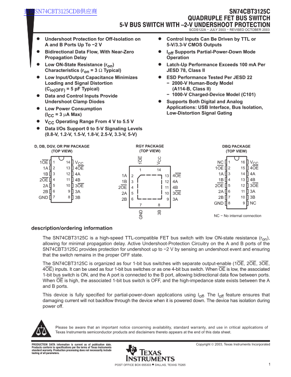
D, DB, DGV, OR PW PACKAGE RGY PACKAGE DBQ PACKAGE (TOP VIEW) (TOP VIEW) (TOP VIEW)
1OE VCC NC VCC 1A 4OE 1OE 4OE 1B 4A 1A 4A
1A 4OE
2OE 4B 1B 4B
2A 3OE 2OE 3OE
2OE 4B
2A 3OE
GND 3B 2B 3B
GND NC
NC − No internal connection
description/ordering information The SN74CBT3125C is a high-speed TTL-compatible FET bus switch with low ON-state resistance (ron), allowing for minimal propagation delay. Active Undershoot-Protection Circuitry on the A and B ports of the SN74CBT3125C provides protection for undershoot up to −2 V by sensing an undershoot event and ensuring that the switch remains in the proper OFF state. The SN74CBT3125C is organized as four 1-bit bus switches with separate output-enable (1OE, 2OE, 3OE, 4OE) inputs. It can be used as four 1-bit bus switches or as one 4-bit bus switch. When OE is low, the associated 1-bit bus switch is ON, and the A port is connected to the B port, allowing bidirectional data flow between ports. When OE is high, the associated 1-bit bus switch is OFF, and the high-impedance state exists between the A and B ports. This device is fully specified for partial-power-down applications using Ioff. The Ioff feature ensures that damaging current will not backflow through the device when it is powered down. The device has isolation during power off.
Please be aware that an important notice concerning availability, standard warranty, and use in critical applications of Texas Instruments semiconductor products and disclaimers thereto appears at the end of this data sheet.
!"#$ % &'!!( $ #% )'*+ &#$ ,#$(- Copyright 2003, Texas Instruments Incorporated
1POST OFFICE BOX 655303 • DALLAS, TEXAS 75265
Page Summary Contents For Texas Instruments SN74CBT3125C Data Sheet
Manual Details
| Brand | Texas Instruments |
|---|---|
| Pages | 15 |
| File Size | 404.19 KB |
| Published | June 21, 2026 |
Enter the captcha to get the download link:
