Texas Instruments SN74ALVCH162601 Data Sheet
Summary
The SN74ALVCH162601 is a versatile 18-bit Universal Bus Transceiver designed for robust data communication across various digital systems. It expertly combines D-type latches and flip-flops, allowing data transmission in transparent, latched, clocked, or clock-enabled modes (A-to-B and B-to-A). This comprehensive manual provides engineers with detailed technical specifications, functional diagrams, operating parameters, and application guidelines needed to design reliable digital bus solutions ranging from 1.65V to 3.6V.
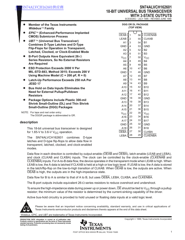
Page 1 Text Content
查询SN74ALVCH162601供应商 SN74ALVCH162601
18-BIT UNIVERSAL BUS TRANSCEIVER
WITH 3-STATE OUTPUTS SCES026G – JULY 1995 – REVISED JUNE 1999 Member of the Texas Instruments DGG OR DL PACKAGE (TOP VIEW)
Widebus Family EPIC (Enhanced-Performance Implanted
OEAB CLKENAB
CMOS) Submicron Process
LEAB CLKAB
UBT (Universal Bus Transceiver)
Combines D-Type Latches and D-Type
GND GND
Flip-Flops for Operation in Transparent,
Latched, Clocked, or Clock-Enabled Mode
B-Port Outputs Have Equivalent 26-Ω
VCC VCC
Series Resistors, So No External Resistors
Are Required
ESD Protection Exceeds 2000 V Per A6 B6 MIL-STD-883, Method 3015; Exceeds 200 V GND GND Using Machine Model (C = 200 p F, R = 0) A7 B7
Latch-Up Performance Exceeds 250 m A Per A8 B8 JESD 17 A9 B9 A10 B10
Bus Hold on Data Inputs Eliminates the
Need for External Pullup/Pulldown
Resistors
GND GND
Package Options Include Plastic 300-mil
Shrink Small-Outline (DL) and Thin Shrink
Small-Outline (DGG) Packages
NOTE: For tape and reel order entry:
VCC VCC
The DGGR package is abbreviated to GR.
description
GND GND This 18-bit universal bus transceiver is designed A18 B18 for 1.65-V to 3.6-V VCC operation. OEBA CLKBA LEBA CLKENBA
The SN74ALVCH162601 combines D-type latches and D-type flip-flops to allow data flow in transparent, latched, clocked, and clock-enabled modes. Data flow in each direction is controlled by output-enable (OEAB and OEBA), latch-enable (LEAB and LEBA), and clock (CLKAB and CLKBA) inputs. The clock can be controlled by the clock-enable (CLKENAB and CLKENBA) inputs. For A-to-B data flow, the device operates in the transparent mode when LEAB is high. When LEAB is low, the A data is latched if CLKAB is held at a high or low logic level. If LEAB is low, the A data is stored in the latch/flip-flop on the low-to-high transition of CLKAB. When OEAB is low, the outputs are active. When OEAB is high, the outputs are in the high-impedance state. Data flow for B to A is similar to that of A to B, but uses OEBA, LEBA, CLKBA, and CLKENBA. The B-port outputs include equivalent 26-Ω series resistors to reduce overshoot and undershoot. To ensure the high-impedance state during power up or power down, OE should be tied to VCC through a pullup resistor; the minimum value of the resistor is determined by the current-sinking capability of the driver. Active bus-hold circuitry is provided to hold unused or floating data inputs at a valid logic level.
Please be aware that an important notice concerning availability, standard warranty, and use in critical applications of Texas Instruments semiconductor products and disclaimers thereto appears at the end of this data sheet.
Widebus, EPIC, and UBT are trademarks of Texas Instruments Incorporated.
Copyright 1999, Texas Instruments Incorporated PRODUCTION DATA information is current as of publication date.
Products conform to specifications per the terms of Texas Instruments standard warranty. Production processing does not necessarily include testing of all parameters.
1POST OFFICE BOX 655303 • DALLAS, TEXAS 75265
Page Summary Contents For Texas Instruments SN74ALVCH162601 Data Sheet
Manual Details
| Brand | Texas Instruments |
|---|---|
| Pages | 11 |
| File Size | 149.04 KB |
| Published | June 17, 2026 |
Enter the captcha to get the download link:

Frequently Asked Questions
What is the operating voltage range of this transceiver?
It operates from 1.65 V to 3.6 V VCC.
What packages are available for the SN74ALVCH162601?
Plastic 300-mil shrink small-outline (DL) and thin shrink small-outline (DGG) packages.
Do B-port outputs need external series resistors?
No, they have equivalent 26-Ω series resistors built-in.
What is the operating temperature range?
It is characterized for operation from –40°C to 85°C.