Texas Instruments SN54LVTH244A Data Sheet
Summary
These octal buffers and line drivers are designed for low-voltage (3.3V) operation while providing robust mixed-mode signal capability up to a 5V TTL interface. Detailed in this manual, the device ensures reliable data transfer through features like hot-insertion support, high ESD protection (exceeding 2000V), and stable mixed-signal operation down to 2.7V. It is an essential component for electronics designers building complex signal buffering or line driving circuits requiring flexible voltage compatibility.
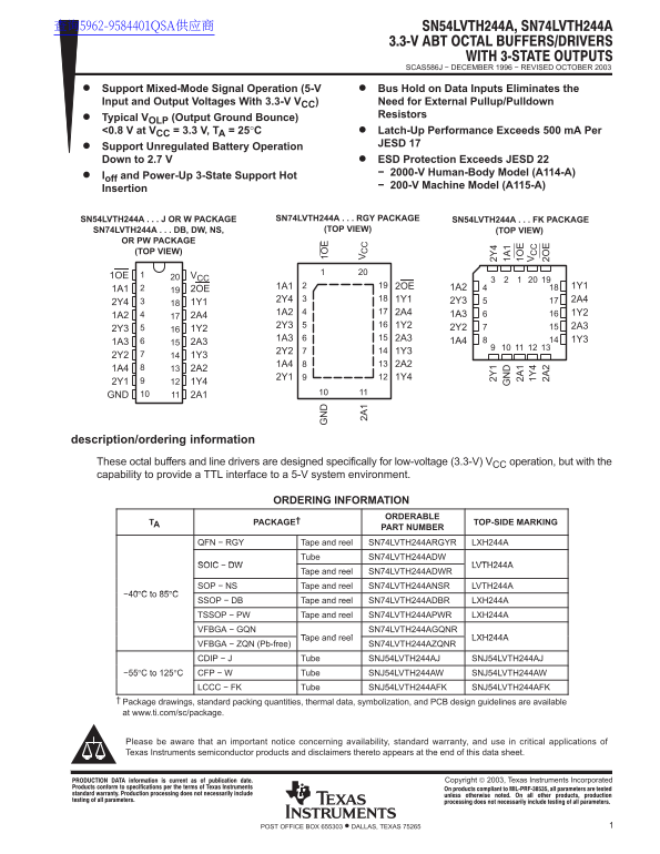
Page 1 Text Content
查询5962-9584401QSA供应商
SCAS586J − DECEMBER 1996 − REVISED OCTOBER 2003
Support Mixed-Mode Signal Operation (5-V Bus Hold on Data Inputs Eliminates the Input and Output Voltages With 3.3-V VCC) Need for External Pullup/Pulldown
Resistors
Typical VOLP (Output Ground Bounce) <0.8 V at VCC = 3.3 V, TA = 25°C Latch-Up Performance Exceeds 500 m A Per
JESD 17
Support Unregulated Battery Operation Down to 2.7 V ESD Protection Exceeds JESD 22
− 2000-V Human-Body Model (A114-A)
Ioff and Power-Up 3-State Support Hot
− 200-V Machine Model (A115-A)
Insertion
SN54LVTH244A J OR W PACKAGE SN74LVTH244A RGY PACKAGE SN54LVTH244A FK PACKAGE
SN74LVTH244A DB, DW, NS, (TOP VIEW) (TOP VIEW)
OR PW PACKAGE (TOP VIEW)
1OE VCC
1A1 2OE 1A2 1Y1
1A1 2OE
2Y1 1Y4 GND 2A1
description/ordering information These octal buffers and line drivers are designed specifically for low-voltage (3.3-V) VCC operation, but with the capability to provide a TTL interface to a 5-V system environment.
ORDERING INFORMATION
ORDERABLE
TA PACKAGE† 2A TOP-SIDE MARKING 1O
PART NUMBER
QFN − RGY Tape and reel SN74LVTH244ARGYR LXH244A
Tube SN74LVTH244ADW
SOIC − DW LVTH244A
Tape and reel SN74LVTH244ADWR
SOP − NS Tape and reel SN74LVTH244ANSR LVTH244A
−40°C to 85°C
SSOP − DB Tape and reel SN74LVTH244ADBR LXH244A TSSOP − PW Tape and reel SN74LVTH244APWR LXH244A VFBGA − GQN SN74LVTH244AGQNR
Tape and reel LXH244A
VFBGA − ZQN (Pb-free) SN74LVTH244AZQNR CDIP − J Tube SNJ54LVTH244AJ SNJ54LVTH244AJ
−55°C to 125°C CFP − W Tube SNJ54LVTH244AW SNJ54LVTH244AW
LCCC − FK Tube SNJ54LVTH244AFK SNJ54LVTH244AFK
Package drawings, standard packing quantities, thermal data, symbolization, and PCB design guidelines are available at www.ti.com/sc/package.
Please be aware that an important notice concerning availability, standard warranty, and use in critical applications of Texas Instruments semiconductor products and disclaimers thereto appears at the end of this data sheet.
!"#$ % &'!!( $ #% )'*+ &#$ ,#$( Copyright 2003, Texas Instruments Incorporated
1POST OFFICE BOX 655303 • DALLAS, TEXAS 75265
Page Summary Contents For Texas Instruments SN54LVTH244A Data Sheet
Manual Details
| Brand | Texas Instruments |
|---|---|
| Pages | 20 |
| File Size | 671.95 KB |
| Published | June 17, 2026 |
Enter the captcha to get the download link:

Frequently Asked Questions
Does this component support both 3.3V and 5V systems?
Yes, it is designed for low-voltage (3.3-V) operation but has the capability to provide a TTL interface to a 5-V system environment.
What resistor arrangement should be used when controlling the Output Enable (OE)?
To keep the outputs in a high-impedance state during power up or down, OE should be tied to V through a pullup resistor. Minimum values are determined by current-sinking capability.
Is it safe to use external resistors with the bus-hold circuitry?
No, using pullup or pulldown resistors with the internal bus-hold circuitry is specifically not recommended.
Can this device withstand repeated power loss and insertion cycles?
Yes, these devices are fully specified for hot-insertion applications and include power-up 3-state circuitry to prevent driver conflict during power cycling.