Texas Instruments SN54LVT245B, SN74LVT245B 3.3-V ABT OCTAL BUS TRANSCEIVERS WITH 3-STATE OUTPUTS User Manual Data Sheet
Summary
Designed for robust data handling, these octal bus transceivers facilitate precise asynchronous communication in demanding 3.3V electronic environments. The manual provides comprehensive technical specifications and design guidelines for SN54LVT245B/SN74LVT245B, enabling mixed-mode signal operation (TTL compatibility) and stable data transfer between buses. Ideal for electronics engineers requiring high reliability, hot-insertion capability, and clear documentation on package options, electrical ratings, and state control features for complex system integration.
Page 1 Text Content
查询SN54LVT245供应商 SN54LVT245B, SN74LVT245B
3.3-V ABT OCTAL BUS TRANSCEIVERS
WITH 3-STATE OUTPUTS SCES004D – JANUARY 1995 – REVISED APRIL 2000
State-of-the-Art Advanced Bi CMOS SN54LVT245B J OR W PACKAGE SN74LVT245B DB, DW, OR PW PACKAGE
Technology (ABT) Design for 3.3-V
(TOP VIEW)
Operation and Low Static-Power Dissipation
DIR VCC
Support Mixed-Mode Signal Operation (5-V
A1 OE
Input and Output Voltages With 3.3-V VCC)
Support Unregulated Battery Operation A3 B2 Down to 2.7 V
A4 B3 Typical VOLP (Output Ground Bounce) A5 B4
<0.8 V at VCC = 3.3 V, TA = 25°C A6 B5
Ioff and Power-Up 3-State Support Hot A7 B6 Insertion A8 B7 GND B8
Latch-Up Performance Exceeds 100 m A Per JESD 78, Class II
ESD Protection Exceeds JESD 22 SN54LVT245B FK PACKAGE
(TOP VIEW)
– 2000-V Human-Body Model (A114-A) – 200-V Machine Model (A115-A) – 1000-V Charged-Device Model (C101) Package Options Include Plastic
Small-Outline (DW), Shrink Small-Outline
(DB), and Thin Shrink Small-Outline (PW)
Packages, Ceramic Chip Carriers (FK), A5 B3 Ceramic Flat (W) Packages, and Ceramic A6 B4 (J) DIPs A7 B5
description These octal bus transceivers are designed specifically for low-voltage (3.3-V) VCC operation, but with the capability to provide a TTL interface
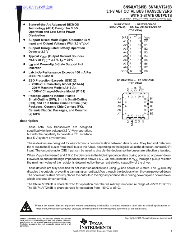
to a 5-V system environment. These devices are designed for asynchronous communication between data buses. They transmit data from the A bus to the B bus or from the B bus to the A bus, depending on the logic level at the direction-control (DIR) input. The output-enable (OE) input can be used to disable the devices so the buses are effectively isolated. When VCC is between 0 and 1.5 V, the device is in the high-impedance state during power up or power down. However, to ensure the high-impedance state above 1.5 V, OE should be tied to VCC through a pullup resistor; the minimum value of the resistor is determined by the current-sinking capability of the driver. These devices are fully specified for hot-insertion applications using Ioff and power-up 3-state. The Ioff circuitry disables the outputs, preventing damaging current backflow through the devices when they are powered down. The power-up 3-state circuitry places the outputs in the high-impedance state during power up and power down, which prevents driver conflict. The SN54LVT245B is characterized for operation over the full military temperature range of –55°C to 125°C. The SN74LVT245B is characterized for operation from –40°C to 85°C.
Please be aware that an important notice concerning availability, standard warranty, and use in critical applications of Texas Instruments semiconductor products and disclaimers thereto appears at the end of this data sheet.
Copyright 2000, Texas Instruments Incorporated UNLESS OTHERWISE NOTED this document contains PRODUCTION
DATA information current as of publication date. Products conform to specifications per the terms of Texas Instruments standard warranty. Production processing does not necessarily include testing of all parameters.
1POST OFFICE BOX 655303 • DALLAS, TEXAS 75265
Page Summary Contents For Texas Instruments SN54LVT245B, SN74LVT245B 3.3-V ABT OCTAL BUS TRANSCEIVERS WITH 3-STATE OUTPUTS User Manual Data Sheet
Manual Details
| Brand | Texas Instruments |
|---|---|
| Pages | 7 |
| File Size | 109.08 KB |
| Published | June 01, 2026 |
Enter the captcha to get the download link:

Frequently Asked Questions
What voltages does the SN54LVT245B support?
It is designed for low-voltage (3.3-V) operation but can provide a TTL interface to a 5-V system environment.
How do I ensure bus isolation during startup or shutdown?
The output-enable (OE) input can be used to disable the devices, effectively isolating the buses. Additionally, OE should be tied to V via a pullup resistor when V is between 0 and 1.5 V.
What does the DIR input control?
The DIR input determines the direction of data flow, allowing data transmission either from A to B or from B to A.
How are hot-insertion applications supported?
The device supports hot insertion and utilizes specialized power-up 3-state circuitry along with I circuitry to prevent damaging current backflow when powered down.