Texas Instruments SN54ABT657A, SN74ABT657A Octal Transceivers with Parity Generators, Checkers, and 3-State Outputs Data Sheet User Manual
Summary
The SN54ABT657A/SN74ABT657A is an octal transceiver designed for robust data transmission, featuring integrated parity generation/checking capabilities and three-state outputs. This manual serves as a comprehensive guide for electrical engineers and designers requiring dependable digital interfaces. It details optimal functional modes (transmit and receive), covering advanced specifications such as superior ESD protection (>2000V), low power dissipation, high immunity, and reliable operation across diverse environmental conditions, ensuring the necessary data integrity for complex circuits.
Page 1 Text Content
查询SN54ABT657A供应商 SN54ABT657A, SN74ABT657A
OCTAL TRANSCEIVERS WITH PARITY GENERATORS/CHECKERS
AND 3-STATE OUTPUTS SCBS192E – JANUARY 1991 – REVISED JUNE 1997
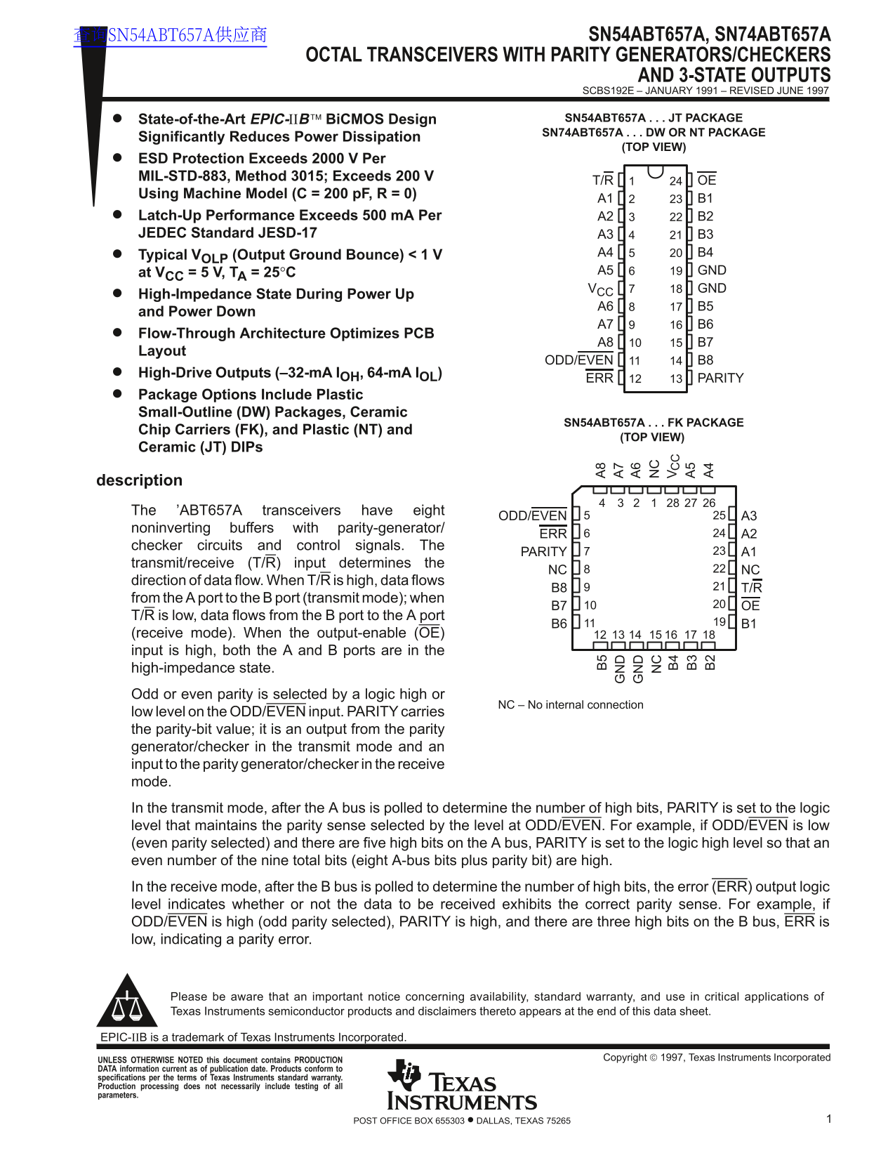
State-of-the-Art EPIC-ΙΙB Bi CMOS Design SN54ABT657A JT PACKAGE SN74ABT657A DW OR NT PACKAGE
Significantly Reduces Power Dissipation
(TOP VIEW)
ESD Protection Exceeds 2000 V Per MIL-STD-883, Method 3015; Exceeds 200 V
T/R OE
Using Machine Model (C = 200 p F, R = 0)
Latch-Up Performance Exceeds 500 m A Per A2 B2 JEDEC Standard JESD-17 A3 B3
Typical VOLP (Output Ground Bounce) < 1 V A4 B4 at VCC = 5 V, TA = 25°C A5 GND VCC GND
High-Impedance State During Power Up
and Power Down
Flow-Through Architecture Optimizes PCB
Layout
ODD/EVEN B8
High-Drive Outputs (–32-m A IOH, 64-m A IOL)
ERR PARITY
Package Options Include Plastic Small-Outline (DW) Packages, Ceramic
SN54ABT657A FK PACKAGE
Chip Carriers (FK), and Plastic (NT) and
(TOP VIEW)
Ceramic (JT) DIPs
description Th ABT657A transceivers have eight
ODD/EVEN A3
noninverting buffers with parity-generator/
ERR A2
checker circuits and control signals. The
PARITY A1
transmit/receive (T/R) input determines the
NC NC
direction of data flow. When T/R is high, data flows
from the A port to the B port (transmit mode); when
B7 OE
T/R is low, data flows from the B port to the A port
(receive mode). When the output-enable (OE) input is high, both the A and B ports are in the high-impedance state. Odd or even parity is selected by a logic high or
NC – No internal connection
low level on the ODD/EVEN input. PARITY carries the parity-bit value; it is an output from the parity generator/checker in the transmit mode and an input to the parity generator/checker in the receive mode. In the transmit mode, after the A bus is polled to determine the number of high bits, PARITY is set to the logic level that maintains the parity sense selected by the level at ODD/EVEN. For example, if ODD/EVEN is low (even parity selected) and there are five high bits on the A bus, PARITY is set to the logic high level so that an even number of the nine total bits (eight A-bus bits plus parity bit) are high. In the receive mode, after the B bus is polled to determine the number of high bits, the error (ERR) output logic level indicates whether or not the data to be received exhibits the correct parity sense. For example, if ODD/EVEN is high (odd parity selected), PARITY is high, and there are three high bits on the B bus, ERR is low, indicating a parity error.
Please be aware that an important notice concerning availability, standard warranty, and use in critical applications of Texas Instruments semiconductor products and disclaimers thereto appears at the end of this data sheet.
EPIC-ΙΙB is a trademark of Texas Instruments Incorporated.
Copyright 1997, Texas Instruments Incorporated UNLESS OTHERWISE NOTED this document contains PRODUCTION
DATA information current as of publication date. Products conform to specifications per the terms of Texas Instruments standard warranty. Production processing does not necessarily include testing of all parameters.
1POST OFFICE BOX 655303 • DALLAS, TEXAS 75265
Page Summary Contents For Texas Instruments SN54ABT657A, SN74ABT657A Octal Transceivers with Parity Generators, Checkers, and 3-State Outputs Data Sheet User Manual
Manual Details
| Brand | Texas Instruments |
|---|---|
| Pages | 9 |
| File Size | 143.89 KB |
| Published | July 12, 2026 |
Enter the captcha to get the download link:

Frequently Asked Questions
What determines the direction of data flow in this transceiver?
Data flows from A to B when T/R is high (transmit mode); it flows from B to A when T/R is low (receive mode).
How should I maintain a high-impedance state above 2.1V V?
The OE input must be tied to V through a pullup resistor, with the minimum value determined by the driver's current-sinking capability.
What are the maximum ESD protection ratings for this device?
The device exceeds 2000 V per MIL-STD-883, Method 3015.
Is this chip suitable for life-support or critical applications?
No. The products are not designed, authorized, or warranted to be suitable for use in life-support devices or other critical applications.