Texas Instruments SN54ALS541, SN74ALS540, SN74ALS541 Data Sheet
Summary
These octal buffers and line drivers are ideal for circuit designers requiring reliable digital signal conditioning and bus driving capabilities. Featuring 3-state outputs and an advanced package layout that places inputs and outputs on opposite sides of the chip, they greatly simplify Printed Circuit Board design. The comprehensive manual provides detailed technical specifications, operational parameters (including true or inverted data options), application guidelines, and ordering information for professional use in digital logic systems.
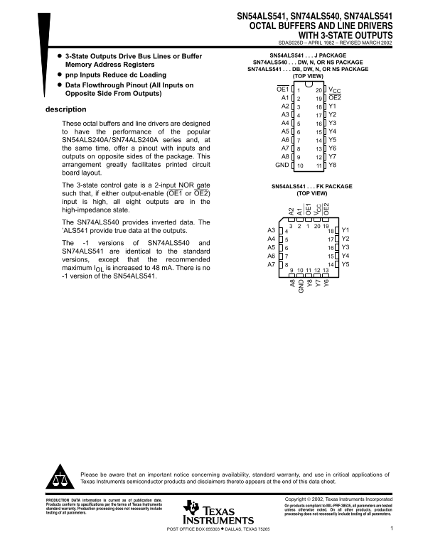
Page 1 Text Content
SN54ALS541, SN74ALS540, SN74ALS541 OCTAL BUFFERS AND LINE DRIVERS
WITH 3-STATE OUTPUTS SDAS025D – APRIL 1982 – REVISED MARCH 2002 3-State Outputs Drive Bus Lines or Buffer SN54ALS541 J PACKAGE
SN74ALS540 DW, N, OR NS PACKAGE
Memory Address Registers
SN74ALS541 DB, DW, N, OR NS PACKAGE
pnp Inputs Reduce dc Loading (TOP VIEW) Data Flowthrough Pinout (All Inputs on
OE1 VCC
Opposite Side From Outputs)
A1 OE2 A2 Y1
description
A3 Y2 These octal buffers and line drivers are designed A4 Y3 to have the performance of the popular A5 Y4 SN54ALS240A/SN74ALS240A series and, at A6 Y5 the same time, offer a pinout with inputs and A7 Y6
outputs on opposite sides of the package. This A8 Y7 arrangement greatly facilitates printed circuit GND Y8 board layout. The 3-state control gate is a 2-input NOR gate SN54ALS541 FK PACKAGE
such that, if either output-enable (OE1 or OE2) (TOP VIEW)
input is high, all eight outputs are in the high-impedance state. The SN74ALS540 provides inverted data. The
’ALS541 provide true data at the outputs. A3 Y1 A4 Y2
The -1 versions of SN74ALS540 and
SN74ALS541 are identical to the standard
versions, except that the recommended
maximum IOL is increased to 48 m A. There is no -1 version of the SN54ALS541.
Please be aware that an important notice concerning availability, standard warranty, and use in critical applications of Texas Instruments semiconductor products and disclaimers thereto appears at the end of this data sheet.
Copyright 2002, Texas Instruments Incorporated PRODUCTION DATA information is current as of publication date.
Products conform to specifications per the terms of Texas Instruments On products compliant to MIL-PRF-38535, all parameters are tested standard warranty. Production processing does not necessarily include unless otherwise noted. On all other products, production testing of all parameters. processing does not necessarily include testing of all parameters.
1POST OFFICE BOX 655303 • DALLAS, TEXAS 75265
Page Summary Contents For Texas Instruments SN54ALS541, SN74ALS540, SN74ALS541 Data Sheet
Manual Details
| Brand | Texas Instruments |
|---|---|
| Pages | 16 |
| File Size | 512.05 KB |
| Published | June 15, 2026 |
Enter the captcha to get the download link:

Frequently Asked Questions
How are the inputs and outputs positioned on the package?
The inputs and outputs are arranged on opposite sides of the package, which greatly facilitates printed circuit board layout.
What condition is required to put all eight outputs into a high-impedance state?
All eight outputs enter a high-impedance state if either output-enable (OE1 or OE2) input is high.
What is the operating temperature range of the device?
The storage temperature range for the device is –65°C to 150°C.
How do the '-1' versions improve performance compared to standard parts?
The -1 versions increase the maximum I up to 48 mA.