# A B C D E F G H I J K L M N O P Q R S T U V W X Y Z

Texas Instruments SN5400/54LS00/54S00, SN7400/74LS00/74S00 User Manual and Specifications

Summary

This comprehensive data sheet details a quad 2-input NAND gate integrated circuit, providing fundamental positive logic for digital designs. The manual serves as a full technical reference, covering electrical specifications, resistor values, and usage guidelines across multiple package types (DIP, SOIC, TSSOP). It details various ordering information to ensure designers can select the ideal component for their specific application and temperature requirements.
📄 Preview PAGE OF 21

Page 1 Text Content

查询SN7400DE4供应商

SDLS025B − DECEMBER 1983 − REVISED OCTOBER 2003

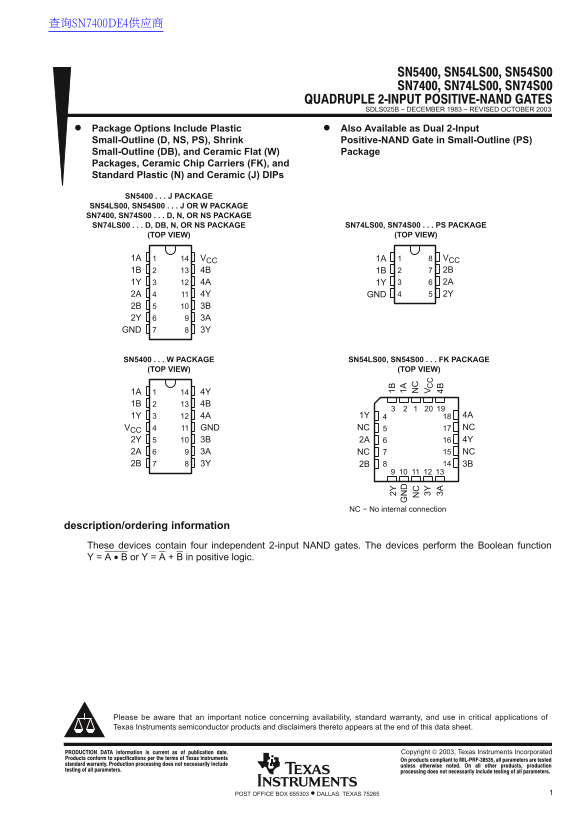
Package Options Include Plastic Also Available as Dual 2-Input Small-Outline (D, NS, PS), Shrink Positive-NAND Gate in Small-Outline (PS) Small-Outline (DB), and Ceramic Flat (W) Package Packages, Ceramic Chip Carriers (FK), and Standard Plastic (N) and Ceramic (J) DIPs

SN5400 J PACKAGE

SN54LS00, SN54S00 J OR W PACKAGE SN7400, SN74S00 D, N, OR NS PACKAGE

SN74LS00 D, DB, N, OR NS PACKAGE SN74LS00, SN74S00 PS PACKAGE

(TOP VIEW) (TOP VIEW)

1A VCC 1A VCC 1B 4B 1B 2B 1Y 4A 1Y 2A 2A 4Y GND 2Y

2B 3B 2Y 3A GND 3Y

SN5400 W PACKAGE SN54LS00, SN54S00 FK PACKAGE (TOP VIEW) (TOP VIEW)

1Y 4A 1Y 4A VCC GND 3Y NC NC 2Y 3B 3A 2A 4B 4Y

2A 3A NC NC 2B 3Y 2B 3B

NC − No internal connection

description/ordering information These devices contain four independent 2-input NAND gates. The devices perform the Boolean function Y = A • B or Y = A + B in positive logic.

Please be aware that an important notice concerning availability, standard warranty, and use in critical applications of Texas Instruments semiconductor products and disclaimers thereto appears at the end of this data sheet.

1POST OFFICE BOX 655303 • DALLAS, TEXAS 75265

Page Summary Contents For Texas Instruments SN5400/54LS00/54S00, SN7400/74LS00/74S00 User Manual and Specifications

Page 1 查询SN7400DE4供应商 SDLS025B − DECEMBER 1983 − REVISED OCTOBER 2003 Package Options Include Plastic Also Available as Dual 2-Input Small-Outline (D, NS, PS), Shrink Positive-NAND Gate in Small-Outline (PS)...
Page 2 SDLS025B − DECEMBER 1983 − REVISED OCTOBER 2003 description/ordering information (continued) ORDERING INFORMATION ORDERABLE TOP-SIDE TA PACKAGE† PART NUMBER MARKING SN7400N SN7400N PDIP − N Tube SN74L...
Page 3 SDLS025B − DECEMBER 1983 − REVISED OCTOBER 2003 schematic ’LS00 ’S00 VCC VCC Resistor values shown are nominal. 3POST OFFICE BOX 655303 • DALLAS, TEXAS 75265
Page 4 SDLS025B − DECEMBER 1983 − REVISED OCTOBER 2003 absolute maximum ratings over operating free-air temperature (unless otherwise noted)† Supply voltage, VCC (see Note 1) 7 V. . . . . . . . . . . . . . ....
Page 5 SDLS025B − DECEMBER 1983 − REVISED OCTOBER 2003 switching characteristics, VCC = 5 V, TA = 25°C (see Figure 1) SN5400 FROM TO SN7400 PARAMETER TEST CONDITIONS UNIT (INPUT) (OUTPUT) MIN TYP MAX t PLH A...
Page 6 SDLS025B − DECEMBER 1983 − REVISED OCTOBER 2003 recommended operating conditions (see Note 5) SN54S00 SN74S00 MIN NOM MAX MIN NOM MAX VCC Supply voltage 4.5 5.5 4.75 5.25 VIH High-level input voltage ...
Page 7 SDLS025B − DECEMBER 1983 − REVISED OCTOBER 2003 PARAMETER MEASUREMENT INFORMATION SERIES 54/74 DEVICES Test RL Test Point Point VCC From Output Under Test (see Note B) From Output (see Note A) 1 kΩ Un...
Page 8 PACKAGE OPTION ADDENDUM www.ti.com 9-Oct-2007 PACKAGING INFORMATION Orderable Device Status Package Package Pins Package Eco Plan Lead/Ball Finish MSL Peak Temp Type Drawing Qty JM38510/00104BCA ACTIV...
Page 9 PACKAGE OPTION ADDENDUM www.ti.com 9-Oct-2007 Orderable Device Status Package Package Pins Package Eco Plan Lead/Ball Finish MSL Peak Temp Type Drawing Qty no Sb/Br) SN74LS00DR ACTIVE SOIC Green (Ro H...
Page 10 PACKAGE OPTION ADDENDUM www.ti.com 9-Oct-2007 Orderable Device Status Package Package Pins Package Eco Plan Lead/Ball Finish MSL Peak Temp Type Drawing Qty SNJ5400J ACTIVE CDIP TBD A42 SNPB for Pkg Ty...
Page 11 PACKAGE MATERIALS INFORMATION www.ti.com 4-Oct-2007 TAPE AND REEL BOX INFORMATION Device Package Pins Site Reel Reel A0 (mm) B0 (mm) K0 (mm) P1 Pin1 Diameter Width (mm) (mm) Quadrant (mm) (mm) SN7400D...
Page 12 PACKAGE MATERIALS INFORMATION www.ti.com 4-Oct-2007 Device Package Pins Site Length (mm) Width (mm) Height (mm) SN7400DR SITE 346.0 346.0 33.0 SN74LS00DBR DB SITE 346.0 346.0 33.0 SN74LS00DR SITE 346....
Page 15 MECHANICAL DATA MLCC006B – OCTOBER 1996 FK (S-CQCC-N**) LEADLESS CERAMIC CHIP CARRIER 28 TERMINAL SHOWN ANO. OF TERMINALS MIN MINMAX MAX B SQ 0.640 0.660 0.495 0.560 NOTES: A. All linear dimensions ar...
Page 20 MECHANICAL DATA MSSO002E – JANUARY 1995 – REVISED DECEMBER 2001 DB (R-PDSO-G**) PLASTIC SMALL-OUTLINE 28 PINS SHOWN Gage Plane Seating Plane 2,00 MAX 0,05 MIN 0,10 PINS ** DIM A MAX 6,506,50 7,50 8,50...
Page 21 IMPORTANT NOTICE Texas Instruments Incorporated and its subsidiaries (TI) reserve the to make corrections, modifications, enhancements, improvements, and other changes to its products and services at ...

Manual Details

Brand Texas Instruments
Pages 21
File Size 717.68 KB
Published June 18, 2026
5 views

Enter the captcha to get the download link:

captcha

Frequently Asked Questions

What is the operating temperature range?

The storage temperature range is -55°C to 150°C. The operating free-air temperature is not explicitly stated but falls within typical application ranges.

Can I use these devices in military or automotive applications without special designation?

No. For military/aerospace, the product must be specifically designated by TI as military-grade. For automotive, they must comply with ISO/TS 16949 requirements and be designated as such.

What is the voltage requirement for the input signals '00 and 'S00?

The input voltage (VCC) ranges from 5.5 V to 7 V depending on the specific package type ('LS00' vs. others).

Which product packages are available?

Available packages include D, DB, N, NS, PS, J, W, FK, and various DIP/SOIC types (e.g., SN7400N, SNJ5400W).