Texas Instruments ADS5521 Specifications and User Guide
Summary
The ADS5521 is a high-performance, 12-bit Analog-to-Digital Converter (ADC) boasting a 105MSPS sample rate. Designed for robust system integration with low power dissipation, it features an internal reference and dedicated S&H stage. This manual details the unit's full technical specifications, pin compatibility across various ADS series chips, and operational parameters. It is ideal for high-speed applications including radar systems, video imaging, medical devices, and advanced communication infrastructure.
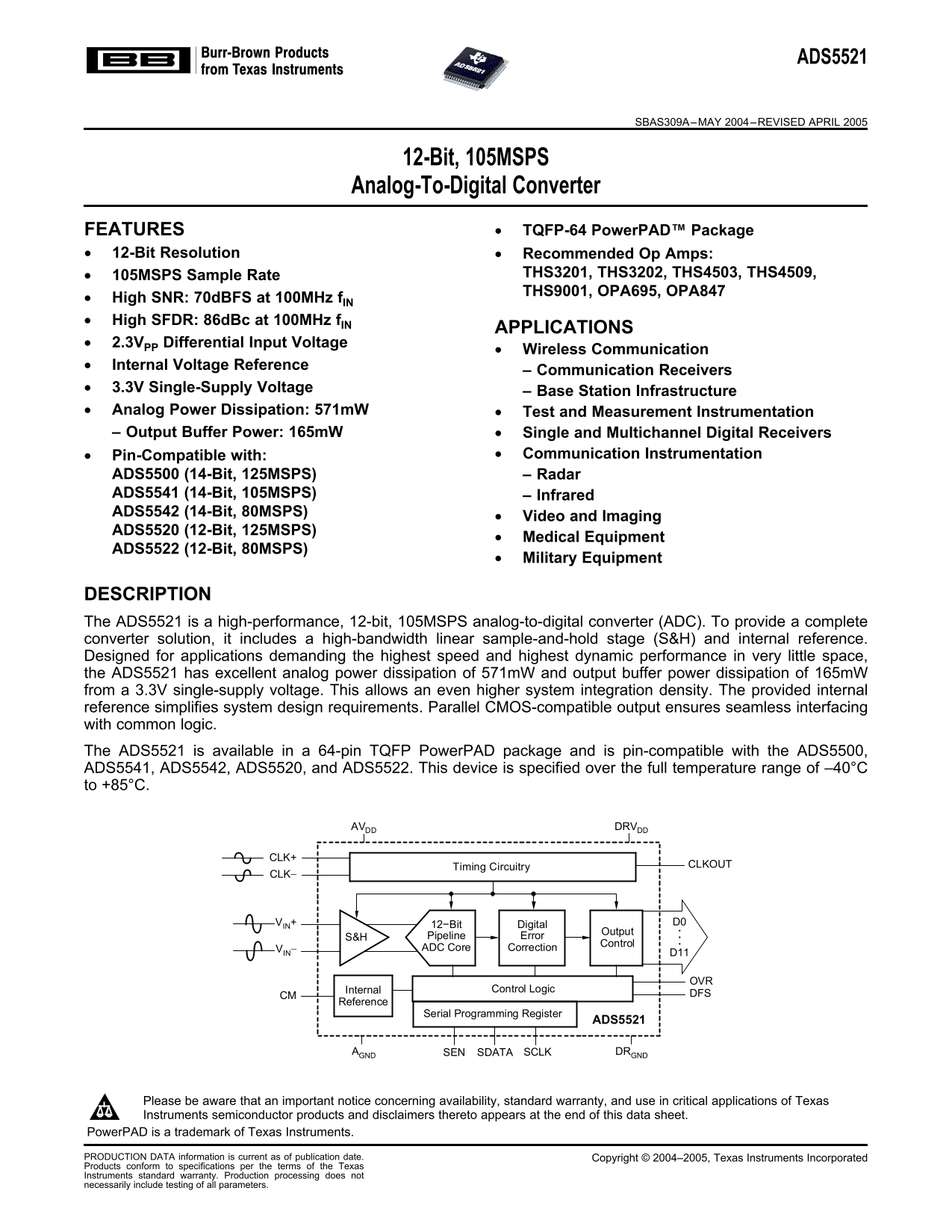
Page 1 Text Content
ADS5521
SBAS309A–MAY 2004–REVISED APRIL
12-Bit, 105MSPS
Analog-To-Digital Converter
FEATURES TQFP-64 Power PAD™ Package
12-Bit Resolution Recommended Op Amps:
105MSPS Sample Rate THS3201, THS3202, THS4503, THS4509,•
THS9001, OPA695, OPA847•
High SNR: 70d BFS at 100MHz f IN
High SFDR: 86d Bc at 100MHz f IN
APPLICATIONS
2.3VPP Differential Input Voltage
Wireless Communication
Internal Voltage Reference
Communication Receivers
3.3V Single-Supply Voltage
Station Infrastructure
Analog Power Dissipation: 571m W Test and Measurement Instrumentation
Output Buffer Power: 165m W Single and Multichannel Digital Receivers
Pin-Compatible with: Communication Instrumentation•
ADS5500 (14-Bit, 125MSPS) Radar
ADS5541 (14-Bit, 105MSPS) Infrared
ADS5542 (14-Bit, 80MSPS)
Video and Imaging
ADS5520 (12-Bit, 125MSPS)
Medical Equipment
ADS5522 (12-Bit, 80MSPS)
Military Equipment
DESCRIPTION
The ADS5521 is high-performance, 12-bit, 105MSPS analog-to-digital converter (ADC). To provide complete
converter solution, it includes high-bandwidth linear sample-and-hold stage (S&H) and internal reference.
Designed for applications demanding the highest speed and highest dynamic performance in very little space,
the ADS5521 has excellent analog power dissipation of 571m W and output buffer power dissipation of 165m W
from 3.3V single-supply voltage. This allows an even higher system integration density. The provided internal
reference simplifies system design requirements. Parallel CMOS-compatible output ensures seamless interfacing
with common logic.
The ADS5521 is available in 64-pin TQFP Power PAD package and is pin-compatible with the ADS5500,
ADS5541, ADS5542, ADS5520, and ADS5522. This device is specified over the full temperature range of –40°C
to +85°C.
AVDD DRVDD
Timing Circuitry CLKOUT
VIN+ 12−Bit Digital D0.
Output
S&H Pipeline Error
Control
VIN− ADC Core Correction
Internal Control Logic
CM DFS
Reference
Serial Programming Register
ADS5521
AGND SDATA SCLK DRGNDSEN
Please be aware that an important notice concerning availability, standard warranty, and use in critical applications of Texas
Instruments semiconductor products and disclaimers thereto appears at the end of this data sheet.
Power PAD is trademark of Texas Instruments.
PRODUCTION DATA information is current as of publication date. Copyright 2004–2005, Texas Instruments Incorporated
Products conform to specifications per the terms of the Texas
Instruments standard warranty. Production processing does not
necessarily include testing of all parameters.
Page Summary Contents For Texas Instruments ADS5521 Specifications and User Guide
Manual Details
| Brand | Texas Instruments |
|---|---|
| Pages | 30 |
| File Size | 587.01 KB |
| Published | July 12, 2026 |
Enter the captcha to get the download link:

Frequently Asked Questions
What are the core specifications of the ADS5521?
It is a 12-bit, 105MSPS analog-to-digital converter packaged in a TQFP-64 PowerPAD package.
Is this model compatible with other Texas Instruments ADC boards?
Yes, it is pin-compatible with models such as the ADS5500, ADS5542, and ADS5520.
Are there specific handling requirements when installing the device?
The circuit can be damaged by ESD; users must handle all integrated circuits with appropriate anti-static precautions.