Texas Instruments SN74LVC541 Specifications and User Guide
Summary
This octal buffer/driver is engineered for robust signal conditioning and driving of bus lines or memory address registers in digital circuits. Optimized for operation from 2.7V to 3.6V, it features complementary inputs and outputs for streamlined Printed Circuit Board (PCB) design. The accompanying documentation provides comprehensive details on operational parameters, electrical ratings, and necessary control techniques, making it essential for electronics engineers designing reliable, high-performance systems needing precise signal buffering and state management.
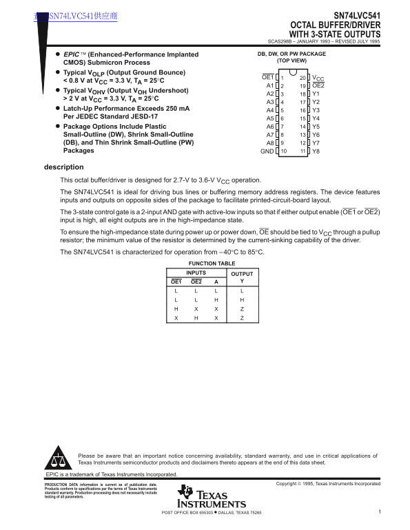
Page 1 Text Content
查询SN74LVC541供应商 SN74LVC541
OCTAL BUFFER/DRIVER WITH 3-STATE OUTPUTS SCAS298B – JANUARY 1993 – REVISED JULY 1995
EPIC (Enhanced-Performance Implanted DB, DW, OR PW PACKAGE (TOP VIEW)
CMOS) Submicron Process Typical VOLP (Output Ground Bounce)
OE1 VCC
< 0.8 V at VCC = 3.3 V, TA = 25°C
A1 OE2
Typical VOHV (Output VOH Undershoot)
> 2 V at VCC = 3.3 V, TA = 25°C
Latch-Up Performance Exceeds 250 m A
Per JEDEC Standard JESD-17
A5 Y4 Package Options Include Plastic A6 Y5
Small-Outline (DW), Shrink Small-Outline A7 Y6 (DB), and Thin Shrink Small-Outline (PW) A8 Y7 Packages GND Y8
description This octal buffer/driver is designed for 2.7-V to 3.6-V VCC operation. The SN74LVC541 is ideal for driving bus lines or buffering memory address registers. The device features inputs and outputs on opposite sides of the package to facilitate printed-circuit-board layout. The 3-state control gate is a 2-input AND gate with active-low inputs so that if either output enable (OE1 or OE2) input is high, all eight outputs are in the high-impedance state. To ensure the high-impedance state during power up or power down, OE should be tied to VCC through a pullup resistor; the minimum value of the resistor is determined by the current-sinking capability of the driver. The SN74LVC541 is characterized for operation from –40°C to 85°C.
FUNCTION TABLE INPUTS OUTPUT OE1 OE2
Please be aware that an important notice concerning availability, standard warranty, and use in critical applications of Texas Instruments semiconductor products and disclaimers thereto appears at the end of this data sheet.
EPIC is a trademark of Texas Instruments Incorporated.
Copyright 1995, Texas Instruments Incorporated PRODUCTION DATA information is current as of publication date.
Products conform to specifications per the terms of Texas Instruments standard warranty. Production processing does not necessarily include testing of all parameters.
1POST OFFICE BOX 655303 • DALLAS, TEXAS 75265
Page Summary Contents For Texas Instruments SN74LVC541 Specifications and User Guide
Manual Details
| Brand | Texas Instruments |
|---|---|
| Pages | 5 |
| File Size | 71.10 KB |
| Published | June 06, 2026 |
Enter the captcha to get the download link:

Frequently Asked Questions
What is required for the high-impedance state when using this buffer?
The output enable (OE) pin must be tied to V through a pullup resistor; the minimum resistor value depends on the current sinking capability.
What is this octal buffer primarily designed for?
It features inputs and outputs ideal for driving bus lines or buffering memory address registers.
What is the typical operating temperature range for this device?
The SN74LVC541 is characterized for operation across a range of –40°C to 85°C.
Can this product be used in life-support or critical applications?
No, Texas Instruments products are not designed, authorized, or warranted for use in life-support systems or other critical applications.