# A B C D E F G H I J K L M N O P Q R S T U V W X Y Z

Texas Instruments OPA3684 Data Sheet

Summary

Discover the OPA3684, a high-performance, low-power triple current-feedback operational amplifier engineered for demanding professional signal processing. This document details its advanced capabilities, including exceptional bandwidth up to 170MHz and minimal drift over temperature. It is designed for critical applications such as broadcast video drivers, multichannel summing amplifiers, and ADC input stages. The manual provides comprehensive technical specifications, making it the ideal component for studio cameras and high-fidelity imaging systems requiring reliable, wideband operation.
📄 Preview PAGE OF 26

Page 1 Text Content

查询DEM-OPA368XD供应商

OPA3684

OPA3684

SBOS241A – MAY 2002 – REVISED SEPTEMBER 2002

Low-Power, Triple Current-Feedback OPERATIONAL AMPLIFIER With Disable FEATURES APPLICATIONS MINIMAL BANDWIDTH CHANGE VERSUS GAIN RGB LINE DRIVERS

170MHz BANDWIDTH: G = +2 LOW-POWER BROADCAST VIDEO DRIVERS > 120MHz BANDWIDTH TO GAIN > +10 EQUALIZING FILTERS LOW DISTORTION: < –82d Bc at 5MHz MULTICHANNEL SUMMING AMPLIFIERS HIGH OUTPUT CURRENT: 120m A PROFESSIONAL CAMERAS SINGLE +5V TO +12V SUPPLY OPERATION ADC INPUT DRIVERS DUAL ±2.5V TO ±6.0V SUPPLY OPERATION LOW SUPPLY CURRENT: 1.7m A/ch LOW SHUTDOWN CURRENT: 100µA/ch

have greater bandwidth, and low-power line drivers to meet the

DESCRIPTION

demanding requirements of studio cameras and broadcast video.

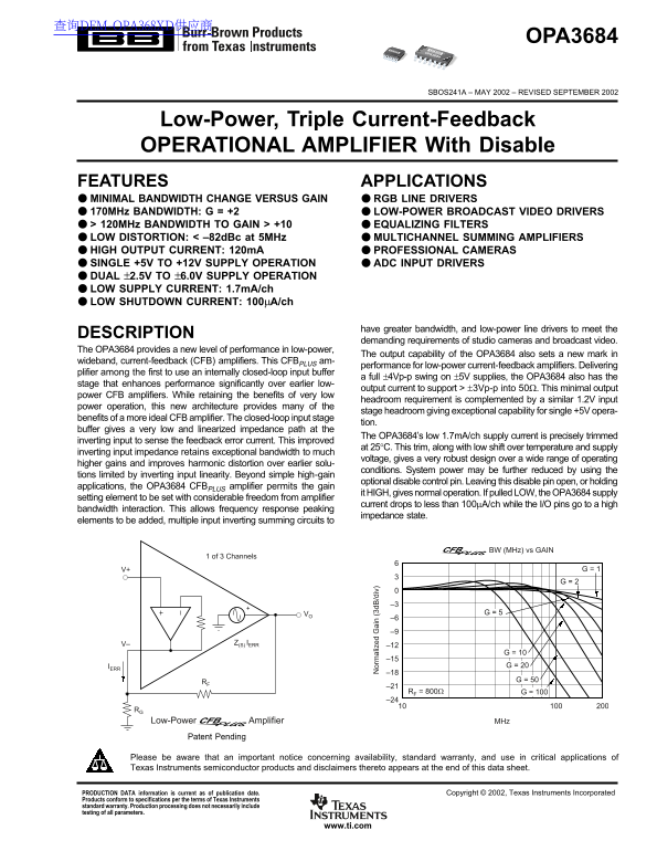
The OPA3684 provides a new level of performance in low-power,

The output capability of the OPA3684 also sets a new mark in

wideband, current-feedback (CFB) amplifiers. This CFBPLUS am-

performance for low-power current-feedback amplifiers. Delivering

plifier among the first to use an internally closed-loop input buffer

or al iz ed ai (3 d B /d iv a full ±4Vp-p swing on ±5V supplies, the OPA3684 also has the

stage that enhances performance significantly over earlier low-

output current to support > ±3Vp-p into 50Ω. This minimal output

power CFB amplifiers. While retaining the benefits of very low

headroom requirement is complemented by a similar 1.2V input

power operation, this new architecture provides many of the

stage headroom giving exceptional capability for single +5V opera-

benefits of a more ideal CFB amplifier. The closed-loop input stage

tion.

buffer gives a very low and linearized impedance path at the

The OPA3684’s low 1.7m A/ch supply current is precisely trimmed

inverting input to sense the feedback error current. This improved

at 25°C. This trim, along with low shift over temperature and supply

inverting input impedance retains exceptional bandwidth to much

voltage, gives a very robust design over a wide range of operating

higher gains and improves harmonic distortion over earlier solu-

conditions. System power may be further reduced by using the

tions limited by inverting input linearity. Beyond simple high-gain

optional disable control pin. Leaving this disable pin open, or holding

applications, the OPA3684 CFBPLUS amplifier permits the gain

it HIGH, gives normal operation. If pulled LOW, the OPA3684 supply

setting element to be set with considerable freedom from amplifier

current drops to less than 100µA/ch while the I/O pins go to a high

bandwidth interaction. This allows frequency response peaking

impedance state.

elements to be added, multiple input inverting summing circuits to

BW (MHz) vs GAIN

1 of 3 Channels

VO G = 5

V– Z(S) IERR

IERR G = 20

RF G = 50

–21 RF = 800Ω G = 100 –24

RG Low-Power Amplifier MHz

Patent Pending

Please be aware that an important notice concerning availability, standard warranty, and use in critical applications of Texas Instruments semiconductor products and disclaimers thereto appears at the end of this data sheet.

PRODUCTION DATA information is current as of publication date. Copyright © 2002, Texas Instruments Incorporated Products conform to specifications per the terms of Texas Instruments standard warranty. Production processing does not necessarily include testing of all parameters.

www.ti.com

Page Summary Contents For Texas Instruments OPA3684 Data Sheet

Page 1 查询DEM-OPA368XD供应商 OPA3684 OPA3684 SBOS241A – MAY 2002 – REVISED SEPTEMBER 2002 Low-Power, Triple Current-Feedback OPERATIONAL AMPLIFIER With Disable FEATURES APPLICATIONS MINIMAL BANDWIDTH CHANGE VERS...
Page 2 ABSOLUTE MAXIMUM RATINGS(1) ELECTROSTATIC Power Supply ±6.5VDC DISCHARGE SENSITIVITY Internal Power Dissipation See Thermal Information Differential Input Voltage ±1.2V This integrated circuit can be ...
Page 3 ELECTRICAL CHARACTERISTICS: VS = ±5V Boldface limits are tested at +25°C. RF = 800Ω, RL = 100Ω, and G = +2, unless otherwise noted. OPA3684ID, IDBQ TYP MIN/MAX OVER TEMPERATURE 0°C to –40°C to MIN/ TE...
Page 4 ELECTRICAL CHARACTERISTICS: VS = +5V Boldface limits are tested at +25°C. RF = 1.0kΩ, RL = 100Ω, and G = +2, unless otherwise noted. OPA3684ID, IDBQ TYP MIN/MAX OVER TEMPERATURE 0°C to –40°C to MIN/ T...
Page 5 TYPICAL CHARACTERISTICS: VS = ±5V At TA = +25°C, G = +2, RF = 800Ω, and RL = 100Ω, unless otherwise noted. ut pu t V ol ta ge 0m /d iv NONINVERTING SMALL-SIGNAL or al iz ed ai (3 d B /d iv ai (d FREQU...
Page 6 TYPICAL CHARACTERISTICS: VS = ±5V (Cont.) ar on ic is to rt io (d c) ar on ic is to rt io (d c) ar on ic is to rt io (d c) At TA = +25°C, G = +2, RF = 800Ω, and RL = 100Ω, unless otherwise noted. HARM...
Page 7 TYPICAL CHARACTERISTICS: VS = ±5V (Cont.) At TA = +25°C, G = +2, RF = 800Ω, and RL = 100Ω, unless otherwise noted. ol ta ge oi se n V /√ z) nd IS 2-TONE, 3RD-ORDER ur re nt oi se p A /√ z) INPUT VOLTA...
Page 8 TYPICAL CHARACTERISTICS: VS = ±5V (Cont.) iff er en tia l G ai In pu t B ia ur re nt (µ om on -M od ej ec tio at io d B iff er en tia l P ha se °) At TA = +25°C, G = +2, RF = 800Ω, and RL = 100Ω, unle...
Page 9 TYPICAL CHARACTERISTICS: VS = ±5V (Cont.) At TA = +25°C, G = +2, RF = 800Ω, and RL = 100Ω, unless otherwise noted. rr or to in al al ue In pu t V ol ta ge 0. 8V /d iv In pu t a nd ut pu t V ol ta ge a...
Page 10 TYPICAL CHARACTERISTICS: VS = +5V ut pu t V ol ta ge 0m /d iv At TA = +25°C, G = +2, RF = 1kΩ, and RL = 100Ω, unless otherwise noted. or al iz ed ai (3 d B /d iv ai (d NONINVERTING SMALL-SIGNAL FREQUE...
Page 11 TYPICAL CHARACTERISTICS: VS = +5V (Cont.) At TA = +25°C, G = +2, RF = 1kΩ, and RL = 100Ω, unless otherwise noted. up pl an ut pu t C ur re nt ar on ic is to rt io (d c) ar on ic is to rt io (d c) HARM...
Page 12 APPLICATIONS INFORMATION mode signal across the input stage, the slew rate for inverting operation is typically higher and the distortion performance is LOW-POWER, CURRENT-FEEDBACK OPERATION slightly ...
Page 13 directly into the blocking capacitor. The source will then see The circuits of Figure 3 and 4 show single-supply operation the 5kΩ load of the biasing network as a load. The gain at +5V. These same ci...
Page 14 LOW-POWER RGB MUX/LINE DRIVER When one channel is shutdown, the feedback network is still present, slightly attenuating the signal and combining in Using the shutdown feature, two OPA3684’s can provid...
Page 15 WIDEBAND PGA FOR ADC DRIVING 0.7Vp-p, diodes across the inputs begin to turn on causing a nonlinear load to the active channel. This will degrade signal Using the 3 channels of the OPA3684, and the sh...
Page 16 The first stage buffers the video DAC output to the first OPERATING SUGGESTIONS 3rd-order filter section. This stage also provides group delay equalization while the 2nd and 3rd stages each give a 3rd...
Page 17 transimpedance gain. The Typical Characteristics show this inverting node voltage. While it is always important to keep open-loop transimpedance response. This is analogous to the inverting node capac...
Page 18 available output voltage and current will always be greater and add the recommended series resistor as close as pos- than that shown in the over temperature specifications since sible to the OPA3684 o...
Page 19 The OPA3684 has an extremely low 3rd-order harmonic The total output spot noise voltage can be computed as the distortion, particularly for light loads and at lower frequen- square root of the sum of ...
Page 20 While the last term, the inverting bias current error, is appear as the impedance looking back into the output, but dominant in this low-gain circuit, the input offset voltage will the circuit will st...
Page 21 BOARD LAYOUT GUIDELINES design. Note that a 800Ω feedback resistor, rather than a direct short, is required for the unity-gain follower Achieving optimum performance with a high-frequency am- applicat...
Page 22 INPUT AND ESD PROTECTION The OPA3684 is built using a very high-speed complemen- tary bipolar process. The internal junction breakdown volt- ages are relatively low for these very small geometry devic...
Page 23 PACKAGE DRAWINGS D (R-PDSO-G**) PLASTIC SMALL-OUTLINE PACKAGE 8 PINS SHOWN 0.244 (6,20) 0.008 (0,20) NOM Gage Plane Seating Plane 0.069 (1,75) MAX 0.004 (0,10) PINS ** DIM A MAX A MIN NOTES: A. All li...
Page 24 PACKAGE DRAWINGS (Cont.) DBQ (R-PDSO-G**) PLASTIC SMALL-OUTLINE 24 PINS SHOWN 0.008 (0,20) NOM Gage Plane 0.069 (1,75) MAX Seating Plane PINS ** DIM A MAX A MIN NOTES: A. All linear dimensions are in ...
Page 25 PACKAGE OPTION ADDENDUM www.ti.com 22-Feb-2005 PACKAGING INFORMATION Orderable Device Status Package Package Pins Package Eco Plan Lead/Ball Finish MSL Peak Temp Type Drawing Qty OPA3684ID ACTIVE SOIC...
Page 26 IMPORTANT NOTICE Texas Instruments Incorporated and its subsidiaries (TI) reserve the right to make corrections, modifications, enhancements, improvements, and other changes to its products and servic...

Manual Details

Brand Texas Instruments
Pages 26
File Size 454.44 KB
Published June 18, 2026
5 views

Enter the captcha to get the download link:

captcha

Frequently Asked Questions

How can I minimize power consumption using this amplifier?

Set the optional disable control pin LOW to reduce the current draw to less than 100μA/ch.

What operating parameters does the OPA3684 support?

It supports single +5V to +12V supply operation and has an Input Voltage Range of ±1.2V DC.

What advanced signal characteristics does this amplifier provide?

It delivers wideband, current-feedback (CFB) performance with low distortion (< –82dBc at 5MHz).

What handling precautions are necessary when installing the integrated circuit?

The device is sensitive to ESD and requires careful handling due to high HBM and CDM ratings.