# A B C D E F G H I J K L M N O P Q R S T U V W X Y Z

Texas Instruments MPS430X21X1 Data Sheet

Summary

Discover the MSP430 family of ultra-low power microcontrollers, engineered for specialized portable measurements and sensor systems. Featuring a powerful 16-bit RISC core and optimizing maximum battery life through advanced low-power modes, this device excels where efficiency is paramount. The manual details various models (including F210x series) optimized with integrated peripherals like analog comparators and timers. Ideal for engineers developing sophisticated applications such as RF sensor front ends or reliable data acquisition systems requiring swift performance and exceptional power management.
📄 Preview PAGE OF 38

Page 1 Text Content

查询MSP430F2101供应商

SLAS439 − SEPTEMBER 2004

Low Supply Voltage Range 1.8 V to 3.6 V Serial Onboard Programming,

No External Programming Voltage Needed

Ultralow-Power Consumption

Programmable Code Protection by

− Active Mode: 200 µA at 1 MHz, 2.2 V

Security Fuse

− Standby Mode: 0.7 µA − Off Mode (RAM Retention): 0.1 µA Bootstrap Loader in Flash Devices Ultrafast Wake-Up From Standby Mode in Family Members Include: less than 1 µs MSP430F2101: 1KB + 256B Flash Memory

128B RAM

16-Bit RISC Architecture, 65 ns

MSP430F2111: 2KB + 256B Flash Memory

Instruction Cycle Time

128B RAM

Basic Clock Module Configurations:

MSP430F2121: 4KB + 256B Flash Memory

− Internal Frequencies up to 16MHz

256B RAM

− 32-k Hz Crystal

MSP430F2131: 8KB + 256B Flash Memory

− High-Frequency Crystal up to 16MHz

256B RAM

− Resonator

Available in a 20-Pin Plastic Small-Outline

− External Clock Source

Wide Body (SOWB) Package, 20-Pin Plastic

16-Bit Timer_A With Three

Small-Outline Thin (TSSOP) Package,

Capture/Compare Registers

20-Pin TVSOP and 24-Pin QFN

On-Chip Comparator for Analog Signal For Complete Module Descriptions, Refer Compare Function or Slope A/D to the MSP430x2xx Family User’s Guide Conversion

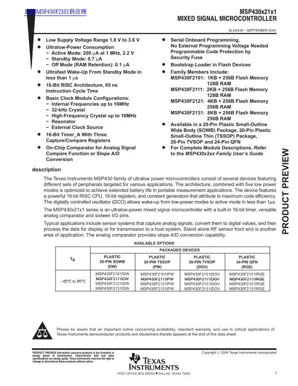
description The Texas Instruments MSP430 family of ultralow power microcontrollers consist of several devices featuring different sets of peripherals targeted for various applications. The architecture, combined with five low power modes is optimized to achieve extended battery life in portable measurement applications. The device features a powerful 16-bit RISC CPU, 16-bit registers, and constant generators that attribute to maximum code efficiency. The digitally controlled oscillator (DCO) allows wake-up from low-power modes to active mode in less than 1µs. The MSP430x21x1 series is an ultralow-power mixed signal microcontroller with a built-in 16-bit timer, versatile analog comparator and sixteen I/O pins. Typical applications include sensor systems that capture analog signals, convert them to digital values, and then process the data for display or for transmission to a host system. Stand alone RF sensor front end is another area of application. The analog comparator provides slope A/D conversion capability.

AVAILABLE OPTIONS

PACKAGED DEVICES

PLASTIC PLASTIC PLASTIC PLASTIC

20-PIN SOWB 20-PIN TSSOP 20-PIN TVSOP 24-PIN QFN (DW) (PW) (DGV) (RGE) MSP430F2101IDW MSP430F2101IPW MSP430F2101IDGV MSP430F2101IRGE MSP430F2111IDW MSP430F2111IPW MSP430F2111IDGV MSP430F2111IRGE

−40°C to 85°C

MSP430F2121IDW MSP430F2121IPW MSP430F2121IDGV MSP430F2121IRGE

MSP430F2131IDW MSP430F2131IPW MSP430F2131IDGV MSP430F2131IRGE

Please be aware that an important notice concerning availability, standard warranty, and use in critical applications of Texas Instruments semiconductor products and disclaimers thereto appears at the end of this data sheet.

1POST OFFICE BOX 655303 • DALLAS, TEXAS 75265

Page Summary Contents For Texas Instruments MPS430X21X1 Data Sheet

Page 1 查询MSP430F2101供应商 SLAS439 − SEPTEMBER 2004 Low Supply Voltage Range 1.8 V to 3.6 V Serial Onboard Programming, No External Programming Voltage Needed Ultralow-Power Consumption Programmable Code Protec...
Page 2 SLAS439 − SEPTEMBER 2004 device pinout DW, PW, or DGV PACKAGE RGE PACKAGE (TOP VIEW) (TOP VIEW) TEST P1.7/TA2/TDO/TDI VCC P1.6/TA1/TDI/TCLK P2.5/CA5 P1.5/TA0/TMS VSS P1.4/SMCLK/TCK XOUT/P2.7/CA7 P1.3/...
Page 3 SLAS439 − SEPTEMBER 2004 Terminal Functions TERMINAL DW, PW, or DGV RGE DESCRIPTION NAME I/O NO. NO. P1.0/TACLK I/O General-purpose digital I/O pin/Timer_A, clock signal TACLK input P1.1/TA0 I/O Gener...
Page 4 SLAS439 − SEPTEMBER 2004 short-form description CPU The MSP430 CPU has a 16-bit RISC architecture Program Counter PC/R0 that is highly transparent to the application. All Stack Pointer SP/R1 operation...
Page 5 SLAS439 − SEPTEMBER 2004 operating modes The MSP430 has one active mode and five software selectable low-power modes of operation. An interrupt event can wake up the device from any of the five low-po...
Page 6 SLAS439 − SEPTEMBER 2004 interrupt vector addresses The interrupt vectors and the power-up starting address are located in the address range of 0FFFFh−0FFE0h. The vector contains the 16-bit address of...
Page 7 SLAS439 − SEPTEMBER 2004 special function registers Most interrupt and module enable bits are collected into the lowest address space. Special function register bits not allocated to a functional purp...
Page 8 SLAS439 − SEPTEMBER 2004 memory organization MSP430F2101 MSP430F2111 MSP430F2121 MSP430F2131 Memory Size 1KB Flash 2KB Flash 4KB Flash 8KB Flash Main: interrupt vector Flash 0FFFFh−0FFE0h 0FFFFh−0FFE0...
Page 9 SLAS439 − SEPTEMBER 2004 peripherals Peripherals are connected to the CPU through data, address, and control busses and can be handled using all instructions. For complete module descriptions, refer t...
Page 10 SLAS439 − SEPTEMBER 2004 comparator_A+ The primary function of the comparator_A module is to support precision slope analog-to-digital conversions, battery-voltage supervision, and monitoring of exter...
Page 11 SLAS439 − SEPTEMBER 2004 peripheral file map PERIPHERALS WITH WORD ACCESS Timer_A Reserved 017Eh Reserved 017Ch Reserved 017Ah Reserved 0178h Capture/compare register TACCR2 0176h Capture/compare regi...
Page 12 SLAS439 − SEPTEMBER 2004 absolute maximum ratings† Voltage applied at VCC to VSS −0.3 V to 4.1 V. . . . . . . . . . . . . . . . . . . . . . . . . . . . . . . . . . . . . . . . . . . . . . . . . . . . ...
Page 13 SLAS439 − SEPTEMBER 2004 electrical characteristics over recommended ranges of supply voltage and operating free-air temperature (unless otherwise noted) supply current (into VCC) excluding external c...
Page 14 SLAS439 − SEPTEMBER 2004 typical supply current (into VCC) characteristics ct iv rr en ct iv rr en VCC − Supply Voltage − V Figure 2. Active mode current vs VCC DCO Frequency − MHz Figure 3. Active mo...
Page 15 SLAS439 − SEPTEMBER 2004 electrical characteristics over recommended ranges of supply voltage and operating free-air temperature (unless otherwise noted) (continued) Schmitt-trigger inputs − Ports P1 ...
Page 16 SLAS439 − SEPTEMBER 2004 electrical characteristics over recommended ranges of supply voltage and operating free-air temperature (unless otherwise noted) (continued) outputs − Ports P1 and P2 PARAMETE...
Page 17 SLAS439 − SEPTEMBER 2004 Ty ic al ig -L ev el tp rr en Ty ic al -L ev el tp rr en electrical characteristics over recommended ranges of supply voltage and operating free-air temperature (unless otherw...
Page 18 SLAS439 − SEPTEMBER 2004 electrical characteristics over recommended ranges of supply voltage and operating free-air temperature (unless otherwise noted) (continued) Timer_A PARAMETER TEST CONDITIONS ...
Page 19 SLAS439 − SEPTEMBER 2004 ef er en ce lt −m electrical characteristics over recommended ranges of supply voltage and operating free-air temperature (unless otherwise noted) (continued) typical characte...
Page 20 SLAS439 − SEPTEMBER 2004 electrical characteristics over recommended ranges of supply voltage and operating free-air temperature (unless otherwise noted) (continued) 0 V VCC To Internal Low Pass Filte...
Page 21 SLAS439 − SEPTEMBER 2004 electrical characteristics over recommended ranges of supply voltage and operating free-air (m in )− (m in )− temperature (unless otherwise noted) (continued) typical characte...
Page 22 SLAS439 − SEPTEMBER 2004 electrical characteristics over recommended ranges of supply voltage and operating free-air temperature (unless otherwise noted) (continued) main DCO characteristics All range...
Page 23 SLAS439 − SEPTEMBER 2004 electrical characteristics over recommended ranges of supply voltage and operating free-air temperature (unless otherwise noted) (continued) DCO drift Temperature drift (Box M...
Page 24 SLAS439 − SEPTEMBER 2004 electrical characteristics over recommended ranges of supply voltage and operating free-air temperature (unless otherwise noted) (continued) wake-up from lower power modes (LP...
Page 25 SLAS439 − SEPTEMBER 2004 electrical characteristics over recommended ranges of supply voltage and operating free-air temperature (unless otherwise noted) (continued) crystal oscillator, LFXT1 PARAMETE...
Page 26 SLAS439 − SEPTEMBER 2004 electrical characteristics over recommended ranges of supply voltage and operating free-air temperature (unless otherwise noted) (continued) typical operating areas for oscill...
Page 27 SLAS439 − SEPTEMBER 2004 electrical characteristics over recommended ranges of supply voltage and operating free-air temperature (unless otherwise noted) (continued) Flash Memory PARAMETER VCC MIN NOM...
Page 28 SLAS439 − SEPTEMBER 2004 APPLICATION INFORMATION Port P1 pin schematic: P1.0 to P1.3, input/output with Schmitt-trigger Px SEL.x CAPD.x Px DIR.x Direction Module Direction 0: Input 1: Output Px OUT.x ...
Page 29 SLAS439 − SEPTEMBER 2004 APPLICATION INFORMATION Port P1 pin schematic: P1.4 to P1.7, input/output with Schmitt-trigger and in-system access features Px REN.x Px OUT.x Px SEL.x 0DVSS Px DIR.x Directio...
Page 30 SLAS439 − SEPTEMBER 2004 APPLICATION INFORMATION Port P2 pin schematic: P2.0 to P2.5, input/output with Schmitt-trigger P2OUT.x CAPD.x P2REN.x P2SEL.x 0DVSS P2DIR.x Direction Module Direction 0: Input...
Page 31 SLAS439 − SEPTEMBER 2004 APPLICATION INFORMATION Port P2 pin schematic: P2.6, input/output with Schmitt-trigger and crystal oscillator input P2OUT.x P2REN.x P2SEL.x CAPD.x 0DVSS P2DIR.x Direction DVSS...
Page 32 SLAS439 − SEPTEMBER 2004 APPLICATION INFORMATION Port P2 pin schematic: P2.7, input/output with Schmitt-trigger and crystal oscillator output P2OUT.x P2REN.x P2SEL.x CAPD.x 0DVSS P2DIR.x Direction DVS...
Page 33 SLAS439 − SEPTEMBER 2004 JTAG fuse check mode MSP430 devices that have the fuse on the TEST terminal have a fuse check mode that tests the continuity of the fuse the first time the JTAG port is access...
Page 34 SLAS439 − SEPTEMBER 2004 MECHANICAL DATA DW (R-PDSO-G**) PLASTIC SMALL-OUTLINE PACKAGE 16 PIN SHOWN 0.299 (7,59) 0.010 (0,25) NOM Gage Plane Seating Plane 0.104 (2,65) MAX PINS ** DIM A MAX A MIN NOTE...
Page 35 SLAS439 − SEPTEMBER 2004 MECHANICAL DATA PW (R-PDSO-G**) PLASTIC SMALL-OUTLINE PACKAGE 14 PINS SHOWN 0,15 NOM Gage Plane Seating Plane 1,20 MAX 0,10 PINS ** DIM A MAX 3,10 5,10 5,10 6,60 7,90 9,80 A M...
Page 36 SLAS439 − SEPTEMBER 2004 MECHANICAL DATA DGV (R-PDSO-G**) PLASTIC SMALL-OUTLINE 24 PINS SHOWN 0,16 NOM Gage Plane Seating Plane 1,20 MAX 0,08 PINS ** DIM A MAX 3,70 5,10 5,103,70 7,90 9,80 11,40 A MIN...
Page 37 SLAS439 − SEPTEMBER 2004 MECHANICAL DATA RGE (S-PQFP-N24) PLASTIC QUAD FLATPACK Pin 1 Index Area Top and Bottom 0,20 REF. Seating Plane 2,55 MAX SQ. Exposed Thermal Die Pad (See Note D) 24X IE NOTES: ...
Page 38 IMPORTANT NOTICE Texas Instruments Incorporated and its subsidiaries (TI) reserve the right to make corrections, modifications, enhancements, improvements, and other changes to its products and servic...

Manual Details

Brand Texas Instruments
Pages 38
File Size 545.17 KB
Published June 18, 2026
1 views

Enter the captcha to get the download link:

captcha

Frequently Asked Questions

What is the minimum operating voltage for this family of microcontrollers?

The low supply voltage range is 1.8 V to 3.6 V.

How fast can the device wake up from a low-power state?

The digitally controlled oscillator allows wake-up from low-power modes in less than 1µs.

What are the different memory configurations available in the MSP430x2xx family?

Configurations include 1KB Flash/128B RAM, 4KB Flash/256B RAM, and 8KB Flash/256B RAM.

Does the device have analog signal processing capabilities?

Yes, it features a versatile analog comparator and provides slope A/D conversion capability.