Texas Instruments DNET2511TA Data Sheet
Summary
The ONET2511TA is a high-performance 2.5 Gbps transimpedance amplifier designed for critical networking applications, including SONET and SDH systems. This device features low input noise, advanced offset cancellation circuitry, and an integrated Received Signal Strength Indicator (RSSI) for optimal link monitoring. The manual provides comprehensive technical details, covering signal path analysis, filter circuit design, and pin configurations necessary for seamless integration into high-speed optical receiver front ends, catering to telecom and defense engineers.
Page 1 Text Content
查询MC33063A-Q1供应商
ONET2511TA
2.5 GBPS TRANSIMPEDANCE AMPLIFIER WITH RSSI
www.ti.com
SLLS622–SEPTEMBER
FEATURES DESCRIPTION
2.5 GHz Bandwidth
The ONET2511TA is high-speed transimpedance
4.0 kΩ Differential Transimpedance amplifier used in SDH/SONET systems with data•
rates up to 2.5Gbps. It features low input referred•
p A/√Hz Typical Input Referred Noise
noise, 2.5GHz bandwidth, 4.0kΩ transimpedance,
m A Maximum Input Current
and received signal strength indicator.
Offset Cancellation
The ONET2511TA device is available in die form and
Received Signal Strength Indication
requires single +3.3V supply. It is very power
Differential CML Data Outputs efficient and dissipates less than m W (typical). It is•
characterized for operations from –40°C to 85°C.•
Single +3.3V Supply
Bare-Die Option
AVAILABLE OPTIONS
TA DIE
APPLICATIONS
–40°C to 85°C ONET2511TAY•
SONET OC-48
SDH STM-16
APD Preamplifier-Receivers
PIN Preamplifier-Receivers
DETAILED DESCRIPTION
BLOCKDIAGRAM
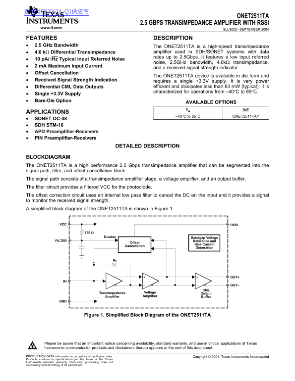
The ONET2511TA is high performance 2.5 Gbps transimpedance amplifier that can be segmented into the
signal path, filter, and offset cancellation block.
The signal path consists of transimpedance amplifier stage, voltage amplifier, and an output buffer.
The filter circuit provides filtered VCC for the photodiode.
The offset correction circuit uses an internal low pass filter to cancel the DC on the input and it provides signal
to monitor the received signal strength.
simplified block diagram of the ONET2511TA is shown in Figure 1.
VCC RSSI
Disable Bandgap Voltage
FILTER Reference and
Offset
Bias Current
Cancellation
Generation
Transimpedance Voltage
Output
Amplifier Amplifier Buffer
Figure 1. Simplified Block Diagram of the ONET2511TA
Please be aware that an important notice concerning availability, standard warranty, and use in critical applications of Texas
Instruments semiconductor products and disclaimers thereto appears at the end of this data sheet.
PRODUCTION DATA information is current as of publication date. Copyright 2004, Texas Instruments Incorporated
Products conform to specifications per the terms of the Texas
Instruments standard warranty. Production processing does not
necessarily include testing of all parameters.
Page Summary Contents For Texas Instruments DNET2511TA Data Sheet
Manual Details
| Brand | Texas Instruments |
|---|---|
| Pages | 12 |
| File Size | 486.09 KB |
| Published | June 02, 2026 |
Enter the captcha to get the download link:

Frequently Asked Questions
How do I disable the offset cancellation loop?
To disable the offset correction circuit, connect the FILTER pin directly to GND.
What voltage supply is required for the ONET2511TA?
The device requires a single +3.3V stable supply (with a tolerance of ± 10%).
Are external components needed for filtering?
Yes, if additional filtering is required beyond the internal mechanism, an external capacitor should be connected to the FILTER pin.
What type of detectors are compatible with this amplifier?
The ONET2511TA can accept input from an anode of PIN or APD preamplifier-receivers.