# A B C D E F G H I J K L M N O P Q R S T U V W X Y Z

Texas Instruments DDC118 Data Sheet

Summary

This comprehensive manual details the DDC118, a high-precision 20-bit octal current input Analog-to-Digital Converter (ADC). Designed to measure ultra-low levels of current from sensors like photodiodes and pyrometers in applications such as CT scanners and chromatography systems. The guide covers critical features including dual $\Delta\Sigma$ integration, programmable full-scale ranges ($\pm 0.5 \text{ppm}$ linearity), and flexible operation in both low-power and high-speed modes, making it ideal for engineers developing complex, multi-device measurement and monitoring systems that require outstanding accuracy over an industrial temperature range.
📄 Preview PAGE OF 30

Page 1 Text Content

查询DDC118供应商

DDC118

SBAS325A − JUNE 2004 − REVISED JUNE 2005

Octal Current Input 20-Bit Analog-To-Digital Converter

FEATURES APPLICATIONS SINGLE-CHIP SOLUTION TO DIRECTLY CT SCANNER DAS MEASURE EIGHT LOW-LEVEL CURRENTS PHOTODIODE SENSORS HIGH PRECISION, TRUE INTEGRATING INFRARED PYROMETER FUNCTION

LIQUID/GAS CHROMATOGRAPHY

INTEGRAL LINEARITY: Protected by US Patent #5841310 ±0.01% of Reading ±0.5ppm of FSR VERY LOW NOISE: 5.2ppm of FSR

LOW POWER: 13.5m W/channel DESCRIPTION

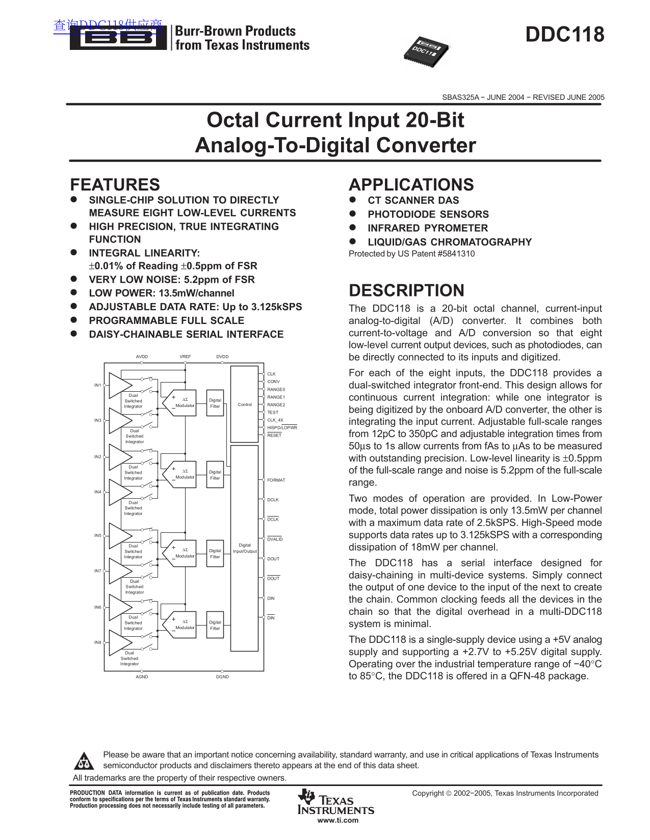
ADJUSTABLE DATA RATE: Up to 3.125k SPS The DDC118 is a 20-bit octal channel, current-input

PROGRAMMABLE FULL SCALE analog-to-digital (A/D) converter. It combines both DAISY-CHAINABLE SERIAL INTERFACE current-to-voltage and A/D conversion so that eight low-level current output devices, such as photodiodes, can

VREF DVDDAVDD be directly connected to its inputs and digitized.

CLK For each of the eight inputs, the DDC118 provides a CONV

IN1 dual-switched integrator front-end. This design allows for

RANGE0

Dual RANGE1

Switched ∆Σ Digital continuous current integration: while one integrator is

Integrator Modulator Filter Control RANGE2

TEST being digitized by the onboard A/D converter, the other is

IN3 CLK_4X

integrating the input current. Adjustable full-scale ranges

HISPD/LOPWR

Switched RESET from 12p C to 350p C and adjustable integration times from

Integrator

50µs to 1s allow currents from f As to µAs to be measured

with outstanding precision. Low-level linearity is ±0.5ppm

Switched ∆Σ Digital of the full-scale range and noise is 5.2ppm of the full-scale Integrator Modulator Filter

FORMAT

range.

DCLK Two modes of operation are provided. In Low-Power

Dual Switched

Integrator mode, total power dissipation is only 13.5m W per channel

with a maximum data rate of 2.5k SPS. High-Speed mode

IN5 supports data rates up to 3.125k SPS with a corresponding

DVALID

Dual Digital

∆Σ Digital dissipation of 18m W per channel.

Switched Input/Output

Integrator Modulator Filter

The DDC118 has a serial interface designed for

DOUT daisy-chaining in multi-device systems. Simply connect

Dual Switched the output of one device to the input of the next to create Integrator

the chain. Common clocking feeds all the devices in the

chain so that the digital overhead in a multi-DDC118

Dual DIN

Switched ∆Σ Digital

Modulator system is minimal.

Integrator Filter

IN8 The DDC118 is a single-supply device using a +5V analog

Dual supply and supporting a +2.7V to +5.25V digital supply. Switched Integrator Operating over the industrial temperature range of −40°C

DGNDAGND to 85°C, the DDC118 is offered in a QFN-48 package.

Please be aware that an important notice concerning availability, standard warranty, and use in critical applications of Texas Instruments semiconductor products and disclaimers thereto appears at the end of this data sheet. All trademarks are the property of their respective owners.

Copyright  2002−2005, Texas Instruments Incorporated

www.ti.com

Page Summary Contents For Texas Instruments DDC118 Data Sheet

Page 1 查询DDC118供应商 DDC118 SBAS325A − JUNE 2004 − REVISED JUNE 2005 Octal Current Input 20-Bit Analog-To-Digital Converter FEATURES APPLICATIONS SINGLE-CHIP SOLUTION TO DIRECTLY CT SCANNER DAS MEASURE EIGHT L...
Page 2 www.ti.com SBAS325A − JUNE 2004 − REVISED JUNE 2005 This integrated circuit can be damaged by ESD. Texas ABSOLUTE MAXIMUM RATINGS(1) Instruments recommends that all integrated circuits be Analog Input...
Page 3 www.ti.com SBAS325A − JUNE 2004 − REVISED JUNE 2005 ELECTRICAL CHARACTERISTICS At TA = +25°C, AVDD = +5V, DVDD = 3V, VREF +4.096V, Range 5 (250p C), and continuous mode operation, unless otherwise not...
Page 4 www.ti.com SBAS325A − JUNE 2004 − REVISED JUNE 2005 ELECTRICAL CHARACTERISTICS (continued) At TA = +25°C, AVDD = +5V, DVDD = 3V, VREF +4.096V, Range 5 (250p C), and continuous mode operation, unless o...
Page 5 www.ti.com SBAS325A − JUNE 2004 − REVISED JUNE 2005 PIN CONFIGURATION Top View QFN DOUT DIN DOUT DIN CLK_4X NC FORMAT NC HISPD/LOPWR RESET RANGE0 TEST DDC118 RANGE1 DGND RANGE2 DGND AGND AGND IN VREF ...
Page 6 www.ti.com is (p of ,r s) SBAS325A − JUNE 2004 − REVISED JUNE 2005 oi se (p pm of ,r s) is (p pm of ,r s) TYPICAL CHARACTERISTICS At TA = +25°C, characterization done with Range 5 (250p C), AVDD = +5V...
Page 7 www.ti.com SBAS325A − JUNE 2004 − REVISED JUNE 2005 TYPICAL CHARACTERISTICS (continued) cc ur en ce ur re nt (m At TA = +25°C, characterization done with Range 5 (250p C), AVDD = +5V, DVDD = 3V, VREF ...
Page 8 www.ti.com SBAS325A − JUNE 2004 − REVISED JUNE 2005 DDC118 in the continuous integration mode, the output of THEORY OF OPERATION the integrators from one side of the inputs will be digitized The block...
Page 9 www.ti.com SBAS325A − JUNE 2004 − REVISED JUNE 2005 The digital interface of the DDC118 provides the digital implement the integration cycle. The timing relationships results via a synchronous serial ...
Page 10 www.ti.com SBAS325A − JUNE 2004 − REVISED JUNE 2005 SINTA SINTB SREF1 SREF2 SRESET SA/D1A Configuration of Wait Convert Wait Convert Integrate Integrator VREF Integrator Voltage Output Figure 4. Basic...
Page 11 www.ti.com SBAS325A − JUNE 2004 − REVISED JUNE 2005 At the completion of an A/D conversion, the charge on the Voltage Reference integration capacitor (CF) is reset with SREF1 and SRESET The external v...
Page 12 www.ti.com in (d SBAS325A − JUNE 2004 − REVISED JUNE 2005 DDC118 Frequency Response Test Mode The frequency response of the DDC118 is set by the front When Test Mode is used, the inputs (IN1, IN2, IN3...
Page 13 www.ti.com SBAS325A − JUNE 2004 − REVISED JUNE 2005 DIGITAL INTERFACE High-Speed and Low-Power Modes (HISPD/LOPWR) The digital interface of the DDC118 provides the digital The HISPD/LOPWR input contro...
Page 14 www.ti.com SBAS325A − JUNE 2004 − REVISED JUNE 2005 Conversion Rate The conversion rate of the DDC118 is set by a combination CONV|mbsy of the integration time (determined by the user) and the speed o...
Page 15 www.ti.com SBAS325A − JUNE 2004 − REVISED JUNE 2005 TIMING EXAMPLES measurement cycles are underway. The internal signal mbsy is shown next. Finally, DVALID is given. DVALID Cont Mode goes active low ...
Page 16 www.ti.com SBAS325A − JUNE 2004 − REVISED JUNE 2005 End Integration Side End Integration Side End Integration Side Start Integration Side Start Integration Side Start Integration Side CONV TINT Side S...
Page 17 www.ti.com SBAS325A − JUNE 2004 − REVISED JUNE 2005 Ncont Mode integration ends, DVALID goes low in time t8. This time is Non-continuous mode of operation is intended for Ranges the same as in the con...
Page 18 www.ti.com SBAS325A − JUNE 2004 − REVISED JUNE 2005 Integration Side Start Integration Side AStart End Integration Side Start Integration Side End Integration Side Release State Wait State TINT t17 A/...
Page 19 www.ti.com SBAS325A − JUNE 2004 − REVISED JUNE 2005 Looking at the state diagram, one can see that the CONV cycle CONV signal with TINT = 512 CLK periods. Care pattern needed to generate a given state...
Page 20 www.ti.com SBAS325A − JUNE 2004 − REVISED JUNE 2005 Changing Between Modes Changing from the ncont to cont mode occurs when TINT Changing from the cont to ncont mode occurs whenever is increased so th...
Page 21 www.ti.com SBAS325A − JUNE 2004 − REVISED JUNE 2005 DATA FORMAT (FORMAT) DATA RETRIEVAL The serial output data is provided in an offset binary code In both the continuous and non-continuous modes of a...
Page 22 www.ti.com SBAS325A − JUNE 2004 − REVISED JUNE 2005 DDC118 devices together to minimize wiring. In this mode SPECIAL CONSIDERATIONS of operation, the serial data output is shifted through Cascading Mu...
Page 23 www.ti.com SBAS325A − JUNE 2004 − REVISED JUNE 2005 RETRIEVAL BEFORE CONV TOGGLES NOTE: 128τDCLK is used for FORMAT = low. (CONTINUOUS MODE) where τDCLK is the period of the data clock. For example, D...
Page 24 www.ti.com SBAS325A − JUNE 2004 − REVISED JUNE 2005 RETRIEVAL AFTER CONV TOGGLES of DDC118s that can be daisy-chained together (FORMAT (CONTINUOUS MODE) = high) is calculated by Equation 3: For shorte...
Page 25 www.ti.com SBAS325A − JUNE 2004 − REVISED JUNE 2005 RETRIEVAL BEFORE AND AFTER CONV RETRIEVAL: NONCONTINUOUS MODE TOGGLES (CONTINUOUS MODE) Retrieving in noncontinuous mode is slightly different, For ...
Page 26 www.ti.com SBAS325A − JUNE 2004 − REVISED JUNE 2005 POWER-UP SEQUENCING Prior to power-up, all digital and analog inputs must be low. After the power supplies have settled, release RESET VA after time...
Page 27 www.ti.com SBAS325A − JUNE 2004 − REVISED JUNE 2005 Shielding Analog Signal Paths currents between the PCB traces can exceed the input bias current of the DDC118 if shielding is not implemented. As wi...
Page 28 PACKAGE OPTION ADDENDUM www.ti.com 1-Jul-2005 PACKAGING INFORMATION Orderable Device Status Package Package Pins Package Eco Plan Lead/Ball Finish MSL Peak Temp Type Drawing Qty DDC118IRTCR ACTIVE QFN...
Page 30 IMPORTANT NOTICE Texas Instruments Incorporated and its subsidiaries (TI) reserve the right to make corrections, modifications, enhancements, improvements, and other changes to its products and servic...

Manual Details

Brand Texas Instruments
Pages 30
File Size 379.44 KB
Published July 12, 2026
0 views

Enter the captcha to get the download link:

captcha

Frequently Asked Questions

How can I connect multiple DDC118 units?

They support daisy-chaining; simply connect the DOUT of one device to the DIN of the next unit in the chain.

What are the operating voltage ranges required for the DDC118?

It is a single-supply device using +5V analog and supporting digital supplies from +2.7V to +5.25V.

What is the difference between Low-Power and High-Speed modes?

Low-Power mode operates up to 2.5kSPS with 13.5mW per channel, while High-Speed mode reaches 3.125kSPS at 18mW per channel.

What are the temperature limits for the DDC118?

The package operating temperature range is from -40°C to +85°C.