Texas Instruments CDCM1804 Data Sheet
Summary
The CDCM1804 is an advanced clock distribution buffer designed for reliable, low-skew signal routing. It efficiently takes one differential input and outputs it across three LVPECL lines and a programmable LVCMOS output. Engineered for robust operation from -40°C to 85°C, this component supports various signaling protocols like LVDS and CML. This documentation provides comprehensive technical details, including its multi-stage control settings, voltage biasing options, and input specifications. It is essential for hardware designers building complex systems requiring high performance in clock domain management.
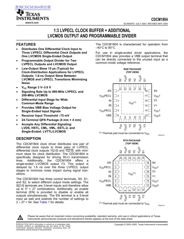
Page 1 Text Content
查询CDCM1804供应商
CDCM1804
www.ti.com
SCAS697E–JULY 2003–REVISED MAY
1:3 LVPECL CLOCK BUFFER ADDITIONAL
LVCMOS OUTPUT AND PROGRAMMABLE DIVIDER
FEATURES The CDCM1804 is characterized for operation from
–40°C to 85°C.•
Distributes One Differential Clock Input to
Three LVPECL Differential Clock Outputs and For use in single-ended driver applications, the
LVCMOS Single-Ended Output CDCM1804 also provides VBB output terminal that One
can be directly connected to the unused input as a•
Programmable Output Divider for Two
common-mode voltage reference.LVPECL
Outputs and LVCMOS Output
Low-Output Skew ps (Typical) for RGE PACKAGE
Clock-Distribution Applications for LVPECL (TOP VIEW)
Outputs; 1.6-ns Output Skew Between
LVCMOS and LVPECL Transitions Minimizing
Noise
VCC Range V–3.6
EN S0
Signaling Rate Up to 800-MHz LVPECL and
200-MHz LVCMOS VDDPECL VDD1
Differential Input Stage for Wide
IN Y1
(1) Common-Mode Range VSS
IN Y1
Provides VBB Bias Voltage Output for
VDDPECL VDD1
Single-Ended Input Signals
Receiver Input Threshold ±75 m V VBB VDD3
24-Terminal QFN Package (4 mm mm)
Accepts Any Differential Signaling:
LVDS, HSTL, CML, VML, SSTL-2, and
Single-Ended: LVTTL/LVCMOS
(1) Thermal pad must be connected to VSS.
DESCRIPTION
RTH PACKAGE The CDCM1804 clock driver distributes one pair of (TOP VIEW)
differential clock inputs to three pairs of LVPECL
differential clock outputs Y[2:0] and Y[2:0], with mini-
mum skew for clock distribution. The CDCM1804 is
specifically designed for driving 50-Ω transmission
lines. Additionally, the CDCM1804 offers
EN S0
single-ended LVCMOS output Y3. This output is
delayed by 1.6 ns over the three LVPECL output VDDPECL VDD1
stages to minimize noise impact during signal tran-
IN Y1
(1) sitions. VSS
IN Y1
The CDCM1804 has three control terminals, S0, S1,
VDDPECL VDD1
and S2, to select different output mode settings. The
S[2:0] terminals are 3-level inputs and therefore allow VBB VDD3
up to combinations. Additionally, an enable
terminal (EN) is provided to disable or enable all
outputs simultaneously. The EN terminal is 3-level
input as well and extends the number of settings to
54. See Table for details. (1) Thermal pad must be connected to VSS.
Please be aware that an important notice concerning availability, standard warranty, and use in critical applications of Texas
Instruments semiconductor products and disclaimers thereto appears at the end of this data sheet.
PRODUCTION DATA information is current as of publication date. Copyright 2003–2005, Texas Instruments Incorporated
Products conform to specifications per the terms of the Texas
Instruments standard warranty. Production processing does not
necessarily include testing of all parameters.
Page Summary Contents For Texas Instruments CDCM1804 Data Sheet
Manual Details
| Brand | Texas Instruments |
|---|---|
| Pages | 24 |
| File Size | 565.08 KB |
| Published | June 18, 2026 |
Enter the captcha to get the download link:

Frequently Asked Questions
What types of differential signals does this chip accept?
It accepts various standards including LVDS, HSTL, CML, VML, and SSTL-2.
How should I properly set up the input termination?
The manual recommends terminating the PCB transmission line before the input, ideally with 100 Ω across the differential pair.
What is the output skew when transitioning between LVCMOS and LVPECL modes?
There is a minimum skew of 1.6 ns between LVCMOS and LVPECL transitions.