Texas Instruments CDC5806 Data Sheet
Summary
This highly functional clock generator utilizes three Phase-Locked Loops (PLLs) to synthesize multiple essential system clocks—including video, audio, CPU, ASIC, USB, and memory card clocks. It ensures reliable operation by generating precise frequencies with low jitter from a single 54 MHz input source. Designed for complex digital television applications, this manual provides comprehensive technical details, covering functional architecture, terminal functions, selection logic, and operating specifications for engineers developing robust multimedia systems.
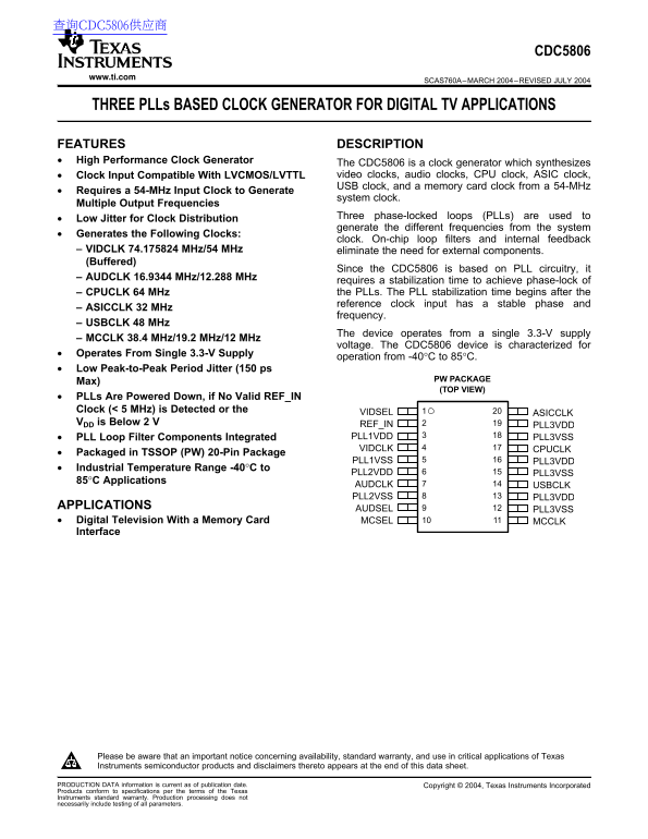
Page 1 Text Content
查询CDC5806供应商
CDC5806
www.ti.com
SCAS760A–MARCH 2004–REVISED JULY
THREE PLLs BASED CLOCK GENERATOR FOR DIGITAL TV APPLICATIONS
FEATURES DESCRIPTION
High Performance Clock Generator
The CDC5806 is clock generator which synthesizes
Clock Input Compatible With LVCMOS/LVTTL video clocks, audio clocks, CPU clock, ASIC clock,•
USB clock, and memory card clock from 54-MHz•
Requires 54-MHz Input Clock to Generate
system clock.Multiple
Output Frequencies
Three phase-locked loops (PLLs) are used to•
Low Jitter for Clock Distribution
generate the different frequencies from the system•
Generates the Following Clocks:
clock. On-chip loop filters and internal feedback
VIDCLK 74.175824 MHz/54 MHz eliminate the need for external components.
(Buffered)
Since the CDC5806 is based on PLL circuitry, it
AUDCLK 16.9344 MHz/12.288 MHz
requires stabilization time to achieve phase-lock of
CPUCLK MHz the PLLs. The PLL stabilization time begins after the–
reference clock input has stable phase and–
ASICCLK MHz
frequency.
USBCLK MHz
The device operates from single 3.3-V supply–
MCCLK 38.4 MHz/19.2 MHz/12 MHz
voltage. The CDC5806 device is characterized for
Operates From Single 3.3-V Supply
operation from -40°C to 85°C.
Low Peak-to-Peak Period Jitter (150 ps
PW PACKAGE
(TOP VIEW)
PLLs Are Powered Down, if No Valid REF_IN
Clock MHz) is Detected or the
VIDSEL ASICCLK
VDD is Below REF_IN
PLL3VDD
PLL Loop Filter Components Integrated PLL1VDD PLL3VSS
VIDCLK CPUCLK
Packaged in TSSOP (PW) 20-Pin Package
PLL1VSS PLL3VDD
Industrial Temperature Range -40°C to
PLL2VDD PLL3VSS
85°C Applications
AUDCLK USBCLK PLL2VSS PLL3VDD
APPLICATIONS AUDSEL
PLL3VSS
Digital Television With Memory Card MCSEL MCCLK
Interface
Please be aware that an important notice concerning availability, standard warranty, and use in critical applications of Texas
Instruments semiconductor products and disclaimers thereto appears at the end of this data sheet.
PRODUCTION DATA information is current as of publication date. Copyright 2004, Texas Instruments Incorporated
Products conform to specifications per the terms of the Texas
Instruments standard warranty. Production processing does not
necessarily include testing of all parameters.
Page Summary Contents For Texas Instruments CDC5806 Data Sheet
Manual Details
| Brand | Texas Instruments |
|---|---|
| Pages | 8 |
| File Size | 98.61 KB |
| Published | June 18, 2026 |
Enter the captcha to get the download link:

Frequently Asked Questions
What type of input clock is required for the CDC5806 to function?
The device needs a 54-MHz reference frequency input (REF_IN) to generate system clocks.
Does the chipset require separate power supplies for each output PLL?
No, it operates from a single 3.3-V supply voltage, although multiple internal power domains (e.g., PLL1VDD, PLL2VDD) are used.
How can I select between different frequencies for outputs like video or audio clocks?
Select inputs such as VIDSEL and AUDSEL are used in conjunction with multiplexers to choose the desired clock frequency.
What safety procedures should be followed when handling this component to prevent damage?
To avoid electrostatic damage, leads should be shorted together or the device must be placed in conductive foam during storage or handling.