Texas Instruments CD74HC137, CD74HCT137, CD54HC237, CD74HC237, CD74HCT237 Data Sheet
Summary
Discover high-performance CMOS decoder/demultiplexer ICs ideal for complex data routing or memory address decoding applications. This guide provides comprehensive technical specifications, including functional block diagrams, detailed timing parameters, low power consumption features, and wide operational temperature ranges down to -55°C. Designed for digital circuit designers and engineers, this manual ensures proper selection and integration of the HC/HCT series logic chips into advanced electronic systems.
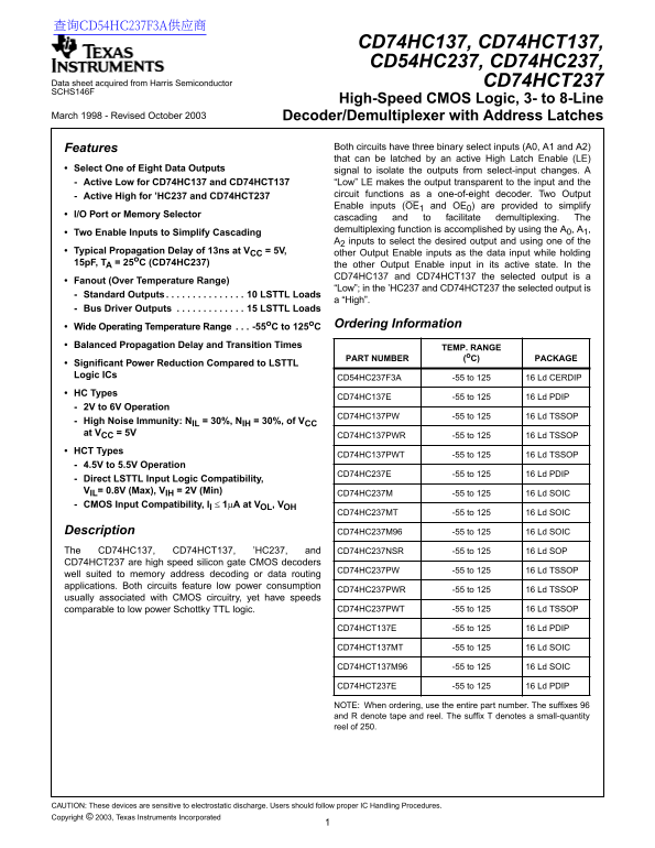
Page 1 Text Content
查询CD54HC237F3A供应商
CD74HC137, CD74HCT137, CD54HC237, CD74HC237,
Data sheet acquired from Harris Semiconductor CD74HCT237 SCHS146F
High-Speed CMOS Logic, 3- to 8-Line
March 1998 - Revised October 2003 Decoder/Demultiplexer with Address Latches
Features Both circuits have three binary select inputs (A0, A1 and A2) that can be latched by an active High Latch Enable (LE)
Select One of Eight Data Outputs signal to isolate the outputs from select-input changes.
Active Low for CD74HC137 and CD74HCT137 “Low” LE makes the output transparent to the input and the
[ /Title
Active High for ’HC237 and CD74HCT237 circuit functions as one-of-eight decoder. Two Output
(CD74 Enable inputs (OE1 and OE0) are provided to simplify
l/O Port or Memory Selector
HC137 cascading and to facilitate demultiplexing. The demultiplexing function is accomplished by using the A0, A1,
Two Enable Inputs to Simplify Cascading
A2 inputs to select the desired output and using one of the
CD74 Typical Propagation Delay of 13ns at VCC = 5V,
other Output Enable inputs as the data input while holding
HCT13 15p F, TA = 25o C (CD74HC237) the other Output Enable input in its active state. In the
7, CD74HC137 and CD74HCT137 the selected output is
Fanout (Over Temperature Range)
“Low”; in the ’HC237 and CD74HCT237 the selected output is
CD74 Standard Outputs . . . . . . . . . . . . . . . 10 LSTTL Loads
a “High”.
HC237 Bus Driver Outputs . . . . . . . . . . . . . 15 LSTTL Loads
Wide Operating Temperature Range . . . -55o C to 125o C Ordering Information
Balanced Propagation Delay and Transition Times
TEMP. RANGE
HCT23
PART NUMBER (o C) PACKAGE
Significant Power Reduction Compared to LSTTL
Logic ICs
CD54HC237F3A -55 to 125 16 Ld CERDIP
/Sub-
HC Types
ject CD74HC137E -55 to 125 16 Ld PDIP
2V to 6V Operation
(High
CD74HC137PW -55 to 125 16 Ld TSSOP
High Noise Immunity: NIL = 30%, NIH = 30%, of VCC
Speed
at VCC = 5V
CD74HC137PWR -55 to 125 16 Ld TSSOP
HCT Types
CD74HC137PWT -55 to 125 16 Ld TSSOP
4.5V to 5.5V Operation
CD74HC237E -55 to 125 16 Ld PDIP
Direct LSTTL Input Logic Compatibility, VIL= 0.8V (Max), VIH = 2V (Min)
CD74HC237M -55 to 125 16 Ld SOIC
CMOS Input Compatibility, Il 1µA at VOL, VOH
CD74HC237MT -55 to 125 16 Ld SOIC
Description CD74HC237M96 -55 to 125 16 Ld SOIC
The CD74HC137, CD74HCT137, ’HC237, and CD74HC237NSR -55 to 125 16 Ld SOP CD74HCT237 are high speed silicon gate CMOS decoders
CD74HC237PW -55 to 125 16 Ld TSSOP
well suited to memory address decoding or data routing applications. Both circuits feature low power consumption
CD74HC237PWR -55 to 125 16 Ld TSSOP
usually associated with CMOS circuitry, yet have speeds
comparable to low power Schottky TTL logic. CD74HC237PWT -55 to 125 16 Ld TSSOP
CD74HCT137E -55 to 125 16 Ld PDIP
CD74HCT137MT -55 to 125 16 Ld SOIC
CD74HCT137M96 -55 to 125 16 Ld SOIC
CD74HCT237E -55 to 125 16 Ld PDIP
NOTE: When ordering, use the entire part number. The suffixes and denote tape and reel. The suffix denotes small-quantity reel of 250.
CAUTION: These devices are sensitive to electrostatic discharge. Users should follow proper IC Handling Procedures. Copyright © 2003, Texas Instruments Incorporated
Page Summary Contents For Texas Instruments CD74HC137, CD74HCT137, CD54HC237, CD74HC237, CD74HCT237 Data Sheet
Manual Details
| Brand | Texas Instruments |
|---|---|
| Pages | 16 |
| File Size | 374.26 KB |
| Published | June 17, 2026 |
Enter the captcha to get the download link:

Frequently Asked Questions
What are these ICs used for?
They function as a one-of-eight decoder, making them suitable for memory address decoding or data routing applications.
What is the operating temperature range?
The specified operation temperature range is wide, ranging from -55°C to 125°C.
How can I connect multiple decoders together?
Using dedicated Output Enable inputs (OE and EE inputs) simplifies cascading and facilitates demultiplexing of the circuits.
What safety precautions are necessary when handling these ICs?
Users must follow proper IC Handling Procedures because these devices are sensitive to electrostatic discharge.