Texas Instruments CD54HC4049, CD74HC4049, CD54HC4050, CD74HC4050 Data Sheet
Summary
These high-speed CMOS logic ICs feature Hex Buffers and Level Translator functionalities for signal integrity across various voltage domains. Ideal for circuit designers, these parts provide robust buffering, inverting, and non-inverting outputs while translating logic levels between different supply voltages (e.g., 5V to 3.3V). The manual details electrical characteristics, advanced input protection, balanced propagation delay, and wide operating temperature ranges (-55°C to 125°C), ensuring reliable performance in demanding applications.
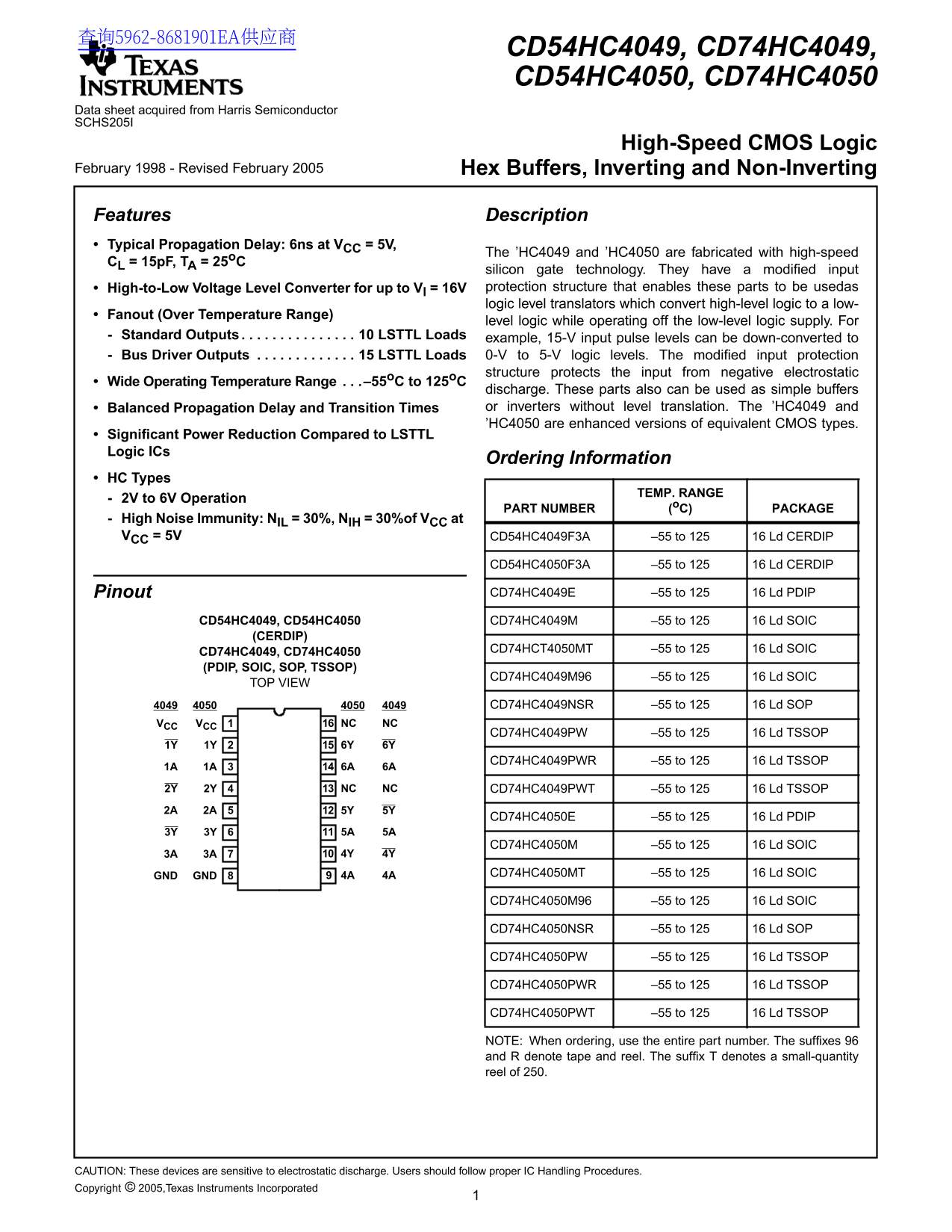
Page 1 Text Content
查询5962-8681901EA供应商
CD54HC4049, CD74HC4049, CD54HC4050, CD74HC4050
Data sheet acquired from Harris Semiconductor SCHS205I
High-Speed CMOS Logic
February 1998 - Revised February 2005 Hex Buffers, Inverting and Non-Inverting
Features Description Typical Propagation Delay: 6ns at VCC = 5V,
The ’HC4049 and ’HC4050 are fabricated with high-speed
CL = 15p F, TA = 25o C
silicon gate technology. They have modified input
[ /Title
High-to-Low Voltage Level Converter for up to Vl 16V protection structure that enables these parts to be usedas
(CD74H
logic level translators which convert high-level logic to low-
C4049, Fanout (Over Temperature Range)
level logic while operating off the low-level logic supply. For
Standard Outputs . . . . . . . . . . . . . . . 10 LSTTL Loads example, 15-V input pulse levels can be down-converted to
CD74H
Bus Driver Outputs . . . . . . . . . . . . . 15 LSTTL Loads 0-V to 5-V logic levels. The modified input protection
structure protects the input from negative electrostatic
/Sub- Wide Operating Temperature Range . . .–55o C to 125o C
discharge. These parts also can be used as simple buffers
ject Balanced Propagation Delay and Transition Times or inverters without level translation. The ’HC4049 and
(High ’HC4050 are enhanced versions of equivalent CMOS types.
Significant Power Reduction Compared to LSTTL
Speed Logic ICs
Ordering Information
HC Types
Logic TEMP. RANGE
2V to 6V Operation
PART NUMBER (o C) PACKAGE
High Noise Immunity: NIL 30%, NIH 30%of VCC at VCC = 5V CD54HC4049F3A –55 to 125 16 Ld CERDIP
CD54HC4050F3A –55 to 125 16 Ld CERDIP
Pinout CD74HC4049E –55 to 125 16 Ld PDIP
CD54HC4049, CD54HC4050 CD74HC4049M –55 to 125 16 Ld SOIC
(CERDIP)
CD74HCT4050MT –55 to 125 16 Ld SOIC
CD74HC4049, CD74HC4050 (PDIP, SOIC, SOP, TSSOP)
CD74HC4049M96 –55 to 125 16 Ld SOIC
TOP VIEW
CD74HC4049NSR –55 to 125 16 Ld SOP
VCC VCC NC NC
CD74HC4049PW –55 to 125 16 Ld TSSOP
CD74HC4049PWR –55 to 125 16 Ld TSSOP
2Y 2Y NC NC CD74HC4049PWT –55 to 125 16 Ld TSSOP
CD74HC4050E –55 to 125 16 Ld PDIP
CD74HC4050M –55 to 125 16 Ld SOIC
GND GND 4A 4A CD74HC4050MT –55 to 125 16 Ld SOIC
CD74HC4050M96 –55 to 125 16 Ld SOIC
CD74HC4050NSR –55 to 125 16 Ld SOP
CD74HC4050PW –55 to 125 16 Ld TSSOP
CD74HC4050PWR –55 to 125 16 Ld TSSOP
CD74HC4050PWT –55 to 125 16 Ld TSSOP
NOTE: When ordering, use the entire part number. The suffixes and denote tape and reel. The suffix denotes small-quantity reel of 250.
CAUTION: These devices are sensitive to electrostatic discharge. Users should follow proper IC Handling Procedures. Copyright © 2005,Texas Instruments Incorporated
Page Summary Contents For Texas Instruments CD54HC4049, CD74HC4049, CD54HC4050, CD74HC4050 Data Sheet
Manual Details
| Brand | Texas Instruments |
|---|---|
| Pages | 7 |
| File Size | 46.57 KB |
| Published | July 22, 2026 |
Enter the captcha to get the download link:

Frequently Asked Questions
What is the specified operating temperature range for these logic ICs?
The wide operating temperature range for these parts is -55°C to 125°C.
Are these chips safe to handle without precautions?
No; caution must be exercised because these devices are sensitive to electrostatic discharge. Proper IC Handling Procedures should be followed.
How do I use the 'HC' series parts if I don't need level conversion function?
The 'HC4049 and 'HC4050 can also be used as simple buffers or inverters without needing level translation.
What is the acceptable supply voltage range for HC types?
For HC Types, the specified operating voltage supply range (VCC) is 2V to 6V.