Page 1
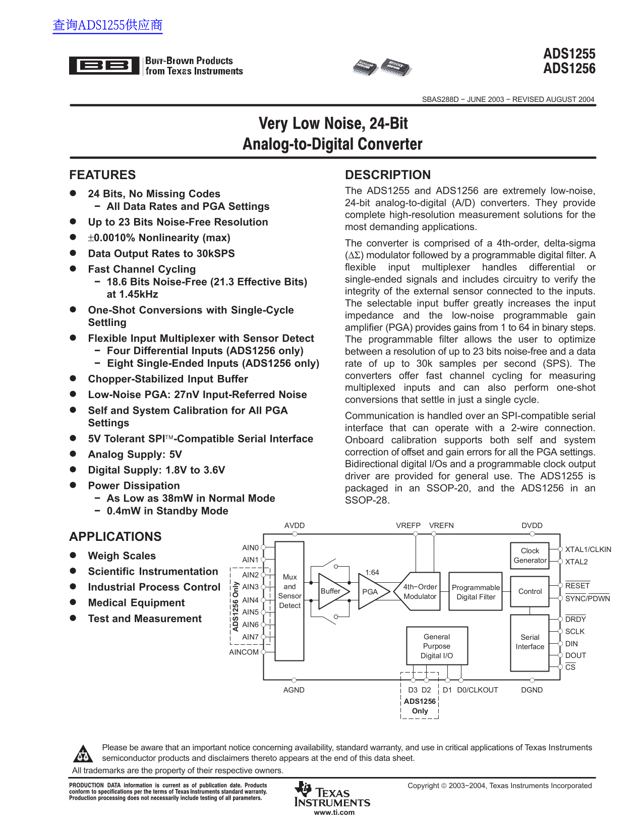
查询ADS1255供应商 SBAS288D − JUNE 2003 − REVISED AUGUST 2004 FEATURES DESCRIPTION The ADS1255 and ADS1256 are extremely low-noise, 24 Bits, No Missing Codes 24-bit analog-to-digital (A/D) converters. They ...
Page 2
www.ti.com SBAS288D − JUNE 2003 − REVISED AUGUST 2004 ORDERING INFORMATION(1) PACKAGE PACKAGE TRANSPORT MEDIA, PRODUCT PACKAGE-LEAD ORDERING NUMBER DESIGNATOR MARKING QUANTITY ADS1255IDBT Tape and Ree...
Page 3
www.ti.com SBAS288D − JUNE 2003 − REVISED AUGUST 2004 ELECTRICAL CHARACTERISTICS All specifications at −40°C to +85°C, AVDD = +5V, DVDD = +1.8V, f CLKIN = 7.68MHz, PGA = 1, and VREF = +2.5V, unless ot...
Page 4
www.ti.com SBAS288D − JUNE 2003 − REVISED AUGUST 2004 ELECTRICAL CHARACTERISTICS (continued) All specifications at −40°C to +85°C, AVDD = +5V, DVDD = +1.8V, f CLKIN = 7.68MHz, PGA = 1, and VREF = +2.5...
Page 5
www.ti.com SBAS288D − JUNE 2003 − REVISED AUGUST 2004 PIN ASSIGNMENTS SSOP PACKAGE AVDD D3 (TOP VIEW) AGND D2 AVDD D1 VREFN D1 AGND D0/CLKOUT VREFP D0/CLKOUT VREFN SCLK AINCOM SCLK VREFP DIN AIN0 DIN ...
Page 6
www.ti.com SBAS288D − JUNE 2003 − REVISED AUGUST 2004 PARAMETER MEASUREMENT INFORMATION t4 t5 t2Lt6 t11 Figure 1. Serial Interface Timing TIMING CHARACTERISTICS FOR FIGURE 1 SYMBOL DESCRIPTION MIN MAX...
Page 7
www.ti.com SBAS288D − JUNE 2003 − REVISED AUGUST 2004 Figure 2. SCLK Reset Timing TIMING CHARACTERISTICS FOR FIGURE 2 SYMBOL DESCRIPTION MIN MAX UNIT t12 SCLK reset pattern, first high pulse τCLKIN(1)...
Page 8
www.ti.com SBAS288D − JUNE 2003 − REVISED AUGUST 2004 er ce to f P op la tio er ce to f P op la tio er ce to f P op la tio TYPICAL CHARACTERISTICS TA = +25°C, AVDD = 5V, DVDD = 1.8V, f CLKIN = 7.68MHz...
Page 9
www.ti.com SBAS288D − JUNE 2003 − REVISED AUGUST 2004 TYPICAL CHARACTERISTICS (continued) er ce to op la tio er ce to f P op la tio er ce nt of op ul tio TA = +25°C, AVDD = 5V, DVDD = 1.8V, f CLKIN = ...
Page 10
IN of www.ti.com SBAS288D − JUNE 2003 − REVISED AUGUST 2004 al ur re nt (m (r s) TYPICAL CHARACTERISTICS (continued) TA = +25°C, AVDD = 5V, DVDD = 1.8V, f CLKIN = 7.68MHz, PGA = 1, and VREF = 2.5V, un...
Page 11
www.ti.com SBAS288D − JUNE 2003 − REVISED AUGUST 2004 OVERVIEW The modulator measures the amplified differential input signal, VIN = (AINP – AINN), against the differential ly The ADS1255 and ADS1256 ...
Page 12
www.ti.com SBAS288D − JUNE 2003 − REVISED AUGUST 2004 NOISE PERFORMANCE Table 2. Effective Number of Bits (ENOB, rms) with Buffer On The ADS1255/6 offer outstanding noise performance that can be optim...
Page 13
www.ti.com SBAS288D − JUNE 2003 − REVISED AUGUST 2004 Table 4. Input Referred Noise (µV, rms) Table 6. Noise-Free Resolution (bits) with Buffer Off with Buffer Off DATA PGA DATA PGA RATE RATE (SPS) (S...
Page 14
www.ti.com SBAS288D − JUNE 2003 − REVISED AUGUST 2004 INPUT MULTIPLEXER However, for optimum analog performance, the following recommendations are made: Figure 6 shows a simplified diagram of the inpu...
Page 15
www.ti.com SBAS288D − JUNE 2003 − REVISED AUGUST 2004 OPEN/SHORT SENSOR DETECTION ANALOG INPUT BUFFER The sensor detect current sources (SDCS) provide a To dramatically increase the input impedance pr...
Page 16
www.ti.com SBAS288D − JUNE 2003 − REVISED AUGUST 2004 PROGRAMMABLE GAIN AMPLIFIER (PGA) repeats with a period of τSAMPLE. This time is a function of the PGA setting as shown in Table 9 along with the ...
Page 17
www.ti.com SBAS288D − JUNE 2003 − REVISED AUGUST 2004 The charging of the input capacitors draws a transient current from the sensor driving the ADS1255/6 inputs. The ly average value of this current ...
Page 18
www.ti.com SBAS288D − JUNE 2003 − REVISED AUGUST 2004 DIGITAL FILTER Table 11 shows the averaging and corresponding data rate for each of the 16 valid DRATE register settings when The programmable low...
Page 19
www.ti.com SBAS288D − JUNE 2003 − REVISED AUGUST 2004 ai (d FREQUENCY RESPONSE The low-pass digital filter sets the overall frequency −6 f DATA 2.5SPS response for the ADS1255/6. The filter response i...
Page 20
www.ti.com ai (d ai (d SBAS288D − JUNE 2003 − REVISED AUGUST 2004 5.76MHz, 7.68MHz, are the same. The digital filter will Table 13. Settling Time vs Data Rate attenuate high-frequency noise on the ADS...
Page 21
www.ti.com SBAS288D − JUNE 2003 − REVISED AUGUST 2004 Settling Time Using the Input Multiplexer Table 14 gives the effective overall throughput (1/t19) when The most efficient way to cycle through the...
Page 22
www.ti.com SBAS288D − JUNE 2003 − REVISED AUGUST 2004 Settling Time Using One-Shot Mode the previous and current input signal and should therefore A dramatic reduction in power consumption can be achi...
Page 23
www.ti.com SBAS288D − JUNE 2003 − REVISED AUGUST 2004 DATA FORMAT CLOCK OUTPUT (D0/CLKOUT) The ADS1255/6 output 24 bits of data in Binary Two’s The clock output pin can be used to clock another device...
Page 24
www.ti.com SBAS288D − JUNE 2003 − REVISED AUGUST 2004 CALIBRATION VIN PGA OFC FSC Output Offset and gain errors can be minimized using the 2VREF ADS1255/6 onboard calibration circuitry. Figure 23 show...
Page 25
www.ti.com SBAS288D − JUNE 2003 − REVISED AUGUST 2004 Self-Calibration Table 20. Self Gain Calibration Timing Self-calibration corrects internal offset and gain errors. DATA RATE PGA SETTING During se...
Page 26
www.ti.com SBAS288D − JUNE 2003 − REVISED AUGUST 2004 System Calibration SERIAL INTERFACE System calibration corrects both internal and external The SPI-compatible serial interface consists of four of...
Page 27
www.ti.com SBAS288D − JUNE 2003 − REVISED AUGUST 2004 DATA READY (DRDY) STANDBY MODE The DRDY output is used as a status signal to indicate The standby mode shuts down all of the analog circuitry when...
Page 28
www.ti.com SBAS288D − JUNE 2003 − REVISED AUGUST 2004 APPLICATIONS INFORMATION the digital pins can help by controlling the trace impedance. When not using the RESET or SYNC/PDWN GENERAL RECOMMENDATIO...
Page 29
www.ti.com SBAS288D − JUNE 2003 − REVISED AUGUST 2004 DIGITAL INTERFACE CONNECTIONS The ADS1255/6 5V tolerant SPI-, QSPI, and ADS1255 MSC12xx or ADS1256 68HC11 MICROWIRE-compatible interface easily ...
Page 30
www.ti.com SBAS288D − JUNE 2003 − REVISED AUGUST 2004 REGISTER MAP The operation of the ADS1255/6 is controlled through a set of registers. Collectively, the registers contain all the information need...
Page 31
www.ti.com SBAS288D − JUNE 2003 − REVISED AUGUST 2004 MUX : Input Multiplexer Control Register (Address 01h) Reset Value = 01h BIT 7 BIT 6 BIT 5 BIT 4 BIT 3 BIT 2 BIT 1 BIT 0 PSEL3 PSEL2 PSEL1 PSEL0 N...
Page 32
www.ti.com SBAS288D − JUNE 2003 − REVISED AUGUST 2004 DRATE: A/D Data Rate (Address 03h) Reset Value = F0h BIT 7 BIT 6 BIT 5 BIT 4 BIT 3 BIT 2 BIT 1 BIT 0 DR7 DR6 DR5 DR4 DR3 DR2 DR1 DR0 The 16 valid ...
Page 33
www.ti.com SBAS288D − JUNE 2003 − REVISED AUGUST 2004 OFC0: Offset Calibration Byte 0, least significant byte (Address 05h) Reset value depends on calibration results. BIT 7 BIT 6 BIT 5 BIT 4 BIT 3 BI...
Page 34
www.ti.com SBAS288D − JUNE 2003 − REVISED AUGUST 2004 COMMAND DEFINITIONS The commands summarized in Table 24 control the operation of the ADS1255/6. All of the commands are stand-alone except for the...
Page 35
www.ti.com SBAS288D − JUNE 2003 − REVISED AUGUST 2004 RDATAC: Read Data Continuous Description: Issue command after DRDY goes low to enter the Read Data Continuous mode. This mode enables the continuo...
Page 36
www.ti.com SBAS288D − JUNE 2003 − REVISED AUGUST 2004 RREG: Read from Registers Description: Output the data from up to 11 registers starting with the register address specified as part of the command...
Page 37
www.ti.com SBAS288D − JUNE 2003 − REVISED AUGUST 2004 SYSOCAL: System Offset Calibration Description: Performs a system offset calibration. The Offset Calibration Register (OFC) is updated after this ...
Page 38
MECHANICAL DATA MSSO002E – JANUARY 1995 – REVISED DECEMBER 2001 DB (R-PDSO-G**) PLASTIC SMALL-OUTLINE 28 PINS SHOWN Gage Plane Seating Plane 2,00 MAX 0,05 MIN 0,10 PINS ** DIM A MAX 6,506,50 7,50 8,50...
Page 39
IMPORTANT NOTICE Texas Instruments Incorporated and its subsidiaries (TI) reserve the right to make corrections, modifications, enhancements, improvements, and other changes to its products and servic...