# A B C D E F G H I J K L M N O P Q R S T U V W X Y Z

Texas Instruments - ADS1100 Data Sheet

Summary

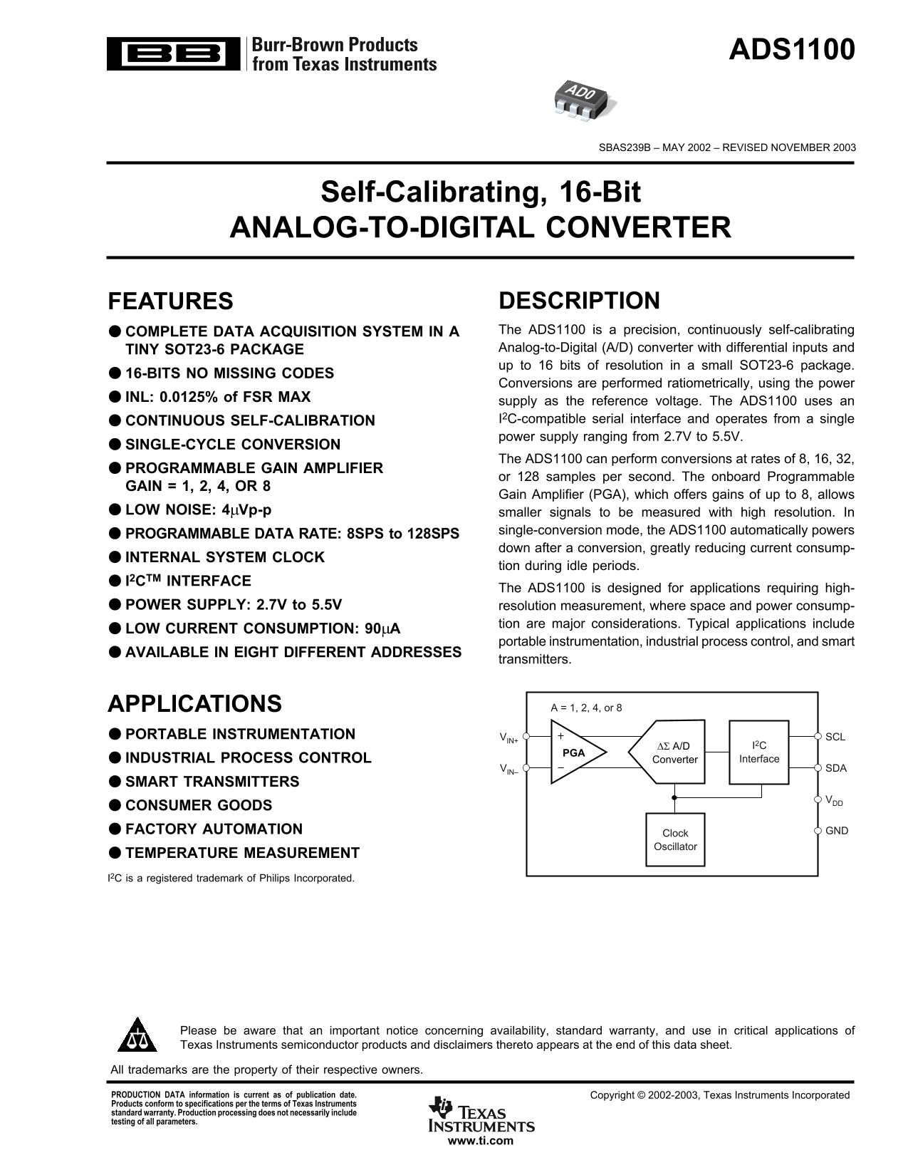
This product is a high-precision, self-calibrating 16-bit Analog-to-Digital Converter (ADC) designed in a compact SOT23-6 package. It offers low noise and customizable performance through an integrated Programmable Gain Amplifier (PGA). This manual provides comprehensive technical specifications, operating parameters, and low-power data acquisition guidance. Ideal for engineers developing portable instrumentation, industrial process control systems, smart transmitters, and factory automation where space, power efficiency, and high resolution are critical requirements.
📄 Preview 📖 Table of Contents Contents PAGE OF 19

Page 1 Text Content

ADS1100

SBAS239B – MAY 2002 – REVISED NOVEMBER 2003

Self-Calibrating, 16-Bit ANALOG-TO-DIGITAL CONVERTER

FEATURES DESCRIPTION COMPLETE DATA ACQUISITION SYSTEM IN A The ADS1100 is a precision, continuously self-calibrating TINY SOT23-6 PACKAGE Analog-to-Digital (A/D) converter with differential inputs and up to 16 bits of resolution in a small SOT23-6 package.

16-BITS NO MISSING CODES

Conversions are performed ratiometrically, using the power

INL: 0.0125% of FSR MAX

supply as the reference voltage. The ADS1100 uses an CONTINUOUS SELF-CALIBRATION I2C-compatible serial interface and operates from a single power supply ranging from 2.7V to 5.5V.

SINGLE-CYCLE CONVERSION

The ADS1100 can perform conversions at rates of 8, 16, 32,

PROGRAMMABLE GAIN AMPLIFIER

or 128 samples per second. The onboard Programmable

GAIN = 1, 2, 4, OR 8

Gain Amplifier (PGA), which offers gains of up to 8, allows

LOW NOISE: 4µVp-p smaller signals to be measured with high resolution. In

single-conversion mode, the ADS1100 automatically powers

PROGRAMMABLE DATA RATE: 8SPS to 128SPS

down after a conversion, greatly reducing current consump-

INTERNAL SYSTEM CLOCK

tion during idle periods.

I2CTM INTERFACE

The ADS1100 is designed for applications requiring high-

POWER SUPPLY: 2.7V to 5.5V resolution measurement, where space and power consump-

tion are major considerations. Typical applications include

LOW CURRENT CONSUMPTION: 90µA

portable instrumentation, industrial process control, and smart

AVAILABLE IN EIGHT DIFFERENT ADDRESSES

transmitters.

APPLICATIONS A = 1, 2, 4, or 8

PORTABLE INSTRUMENTATION VIN+ SCL

INDUSTRIAL PROCESS CONTROL Converter Interface

VIN– SDA

SMART TRANSMITTERS

CONSUMER GOODS FACTORY AUTOMATION Clock GND

Oscillator

TEMPERATURE MEASUREMENT I2C is a registered trademark of Philips Incorporated.

Please be aware that an important notice concerning availability, standard warranty, and use in critical applications of Texas Instruments semiconductor products and disclaimers thereto appears at the end of this data sheet.

All trademarks are the property of their respective owners.

PRODUCTION DATA information is current as of publication date. Copyright © 2002-2003, Texas Instruments Incorporated Products conform to specifications per the terms of Texas Instruments standard warranty. Production processing does not necessarily include testing of all parameters.

www.ti.com

Page Summary Contents For Texas Instruments - ADS1100 Data Sheet

Page 1 ADS1100 SBAS239B – MAY 2002 – REVISED NOVEMBER 2003 Self-Calibrating, 16-Bit ANALOG-TO-DIGITAL CONVERTER FEATURES DESCRIPTION COMPLETE DATA ACQUISITION SYSTEM IN A The ADS1100 is a precision, continuo...
Page 2 ABSOLUTE MAXIMUM RATINGS ELECTROSTATIC VDD to GND –0.3V to +6V Input Current 100m A, Momentary DISCHARGE SENSITIVITY Input Current 10m A, Continuous This integrated circuit can be damaged by ESD. Texa...
Page 3 ELECTRICAL CHARACTERISTICS All specifications at –40°C to +85°C, VDD = 5V, GND = 0V, and all PGAs, unless otherwise noted. ADS1100 PARAMETER CONDITIONS MIN TYP MAX UNITS ANALOG INPUT Full-Scale Input ...
Page 4 TYPICAL CHARACTERISTICS ai rr or ffs et rr or µA At TA = 25°C and VDD = 5V, unless otherwise noted. SUPPLY CURRENT vs TEMPERATURE SUPPLY CURRENT vs I2C BUS FREQUENCY VDD = 5V VDD = 2.7V –40°C Temperat...
Page 5 TYPICAL CHARACTERISTICS (Cont.) At TA = 25°C and VDD = 5V, unless otherwise noted. In te gr al on lin ea rit f F To ta l E rr or oi se p- p, f L TOTAL ERROR vs INPUT SIGNAL INTEGRAL NONLINEARITY vs SU...
Page 6 TYPICAL CHARACTERISTICS (Cont.) At TA = 25°C and VDD = 5V, unless otherwise noted. at at (S DATA RATE vs TEMPERATURE FREQUENCY RESPONSE Data Rate = 8SPS VDD = 2.7V –20 VDD = 5V Data Rate = 8SPS Input ...
Page 7 INPUT SIGNAL DATA RATE NEGATIVE FULL-SCALE –1LSB ZERO +1LSB POSITIVE FULL-SCALE 8SPS 8000H FFFFH 0000H 0001H 7FFFH 16SPS C000H FFFFH 0000H 0001H 3FFFH 32SPS E000H FFFFH 0000H 0001H 1FFFH 128SPS F800H ...
Page 8 Communication on the I2C bus always takes place between Every byte transmitted on the I2C bus, whether it be address two devices, one acting as the master and the other acting or data, is acknowledged...
Page 9 FAST MODE HIGH-SPEED MODE PARAMETER MIN MAX MIN MAX UNITS SCLK Operating Frequency f(SCLK) 0.4 3.4 MHz Bus Free Time Between STOP and START Condition t(BUF) ns Hold Time After Repeated START Condition...
Page 10 When read in single conversion mode, ST/BSY indicates whether READING FROM THE ADS1100 the A/D converter is busy taking a conversion. If ST/BSY is read You can read the output register and the content...
Page 11 A2 A1 A0 R/W D15 D14 D13 D12 D11 D10 D9 D8 …SDA Start By ACK By From ACK By Master ADS1100 ADS1100 Master Frame 1: I2C Slave Address Byte Frame 2: Output Register Upper Byte SCL (Continued) SDA ST/ D7...
Page 12 APPLICATIONS INFORMATION non-multiiple-master I2C peripherals, will work with the ADS1100. The ADS1100 does not perform clock-stretching The sections that follow give example circuits and tips for (i....
Page 13 Note that no pull-up resistor is shown on the SCL line. In this I2C Pull-Up Resistors 1kΩ to 10kΩ (typ.) simple case, the resistor is not needed; the microcontroller can simply leave the line on outpu...
Page 14 Negative input voltages must be level-shifted. A good candi- WHEATSTONE BRIDGE SENSOR date for this function is the Texas Instruments THS4130 The ADS1100 has a fully differential high-impedance input ...
Page 15 Many resistive bridge sensors, such as strain gauges, have If the ADS1100 is driven by an op amp with high voltage very small full-scale output ranges. For these sensors, the supplies, such as ±12V, p...
Page 16 PACKAGE OPTION ADDENDUM www.ti.com 30-Mar-2005 PACKAGING INFORMATION Orderable Device Status Package Package Pins Package Eco Plan Lead/Ball Finish MSL Peak Temp Type Drawing Qty ADS1100A0IDBVR ACTIVE...
Page 17 PACKAGE OPTION ADDENDUM www.ti.com 30-Mar-2005 reasonable steps to provide representative and accurate information but may not have conducted destructive testing or chemical analysis on incoming mater...
Page 19 IMPORTANT NOTICE Texas Instruments Incorporated and its subsidiaries (TI) reserve the right to make corrections, modifications, enhancements, improvements, and other changes to its products and servic...

Manual Details

Brand Texas Instruments
Pages 19
File Size 284.96 KB
Published July 12, 2026
2 views

Enter the captcha to get the download link:

captcha

Frequently Asked Questions

What is the maximum resolution of the ADS1100?

The device offers up to 16 bits of resolution.

What operating voltage range does it support?

It operates from a single power supply ranging from 2.7V to 5.5V.

How fast can the ADS1100 convert samples?

It supports conversion rates of up to 128 samples per second (SPS).

What precautions should be taken when handling the chip?

Electrostatic Discharge (ESD) can damage this integrated circuit, requiring careful handling.