SIEMENS Buzzer BUZ 101L User's Guide
Summary
A high-performance N-channel Silicon Carbide (SiC) power transistor designed for demanding, high-power operation up to 175°C. This essential component features low on-resistance and robust handling of transient currents. The comprehensive manual covers every technical specification, including detailed maximum ratings, dynamic electrical characteristics (e.g., turn-on/off times), thermal impedance modeling, and operational curves for robust design verification. It is the ideal resource for power electronics engineers building reliable circuit designs that require exceptional performance in high-temperature or harsh industrial environments.
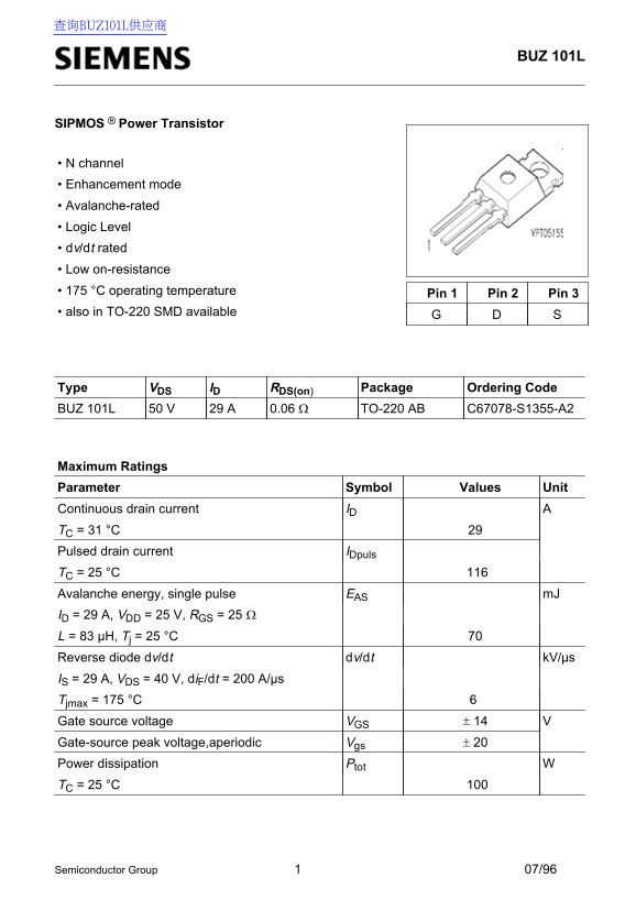
Page 1 Text Content
查询BUZ101L供应商
BUZ 101L
SIPMOS ® Power Transistor
• N channel • Enhancement mode • Avalanche-rated • Logic Level • dv/dt rated • Low on-resistance • 175 °C operating temperature Pin 1 Pin 2 Pin 3 • also in TO-220 SMD available
Type VDS ID RDS(on) Package Ordering Code BUZ 101L 50 V 29 A 0.06 Ω TO-220 AB C67078-S1355-A2
Maximum Ratings Parameter Symbol Values Unit Continuous drain current ID TC = 31 °C Pulsed drain current IDpuls TC = 25 °C Avalanche energy, single pulse EAS m J ID = 29 A, VDD = 25 V, RGS = 25 Ω L = 83 µH, Tj = 25 °C Reverse diode dv/dt dv/dt k V/µs IS = 29 A, VDS = 40 V, di F/dt = 200 A/µs Tjmax = 175 °C
Gate source voltage VGS ± 14 Gate-source peak voltage,aperiodic Vgs ± 20
Power dissipation Ptot TC = 25 °C
Semiconductor Group 07/96
Page Summary Contents For SIEMENS Buzzer BUZ 101L User's Guide
Manual Details
| Brand | Siemens |
|---|---|
| Pages | 9 |
| File Size | 178.23 KB |
| Published | June 04, 2026 |
Enter the captcha to get the download link:

Frequently Asked Questions
What is the maximum continuous drain current (IAD)?
At a temperature of 31°C, the maximum continuous drain current (IAD) is 29 A.
What is the operating temperature range for this transistor?
The operating temperature range is from -55°C to +175°C.
How is the chip resistance rated in terms of thermal performance?
The chip case (thJC) and thermal resistance, chip to ambient (thJA), are both specified with maximum values of 1.5 K/W and 75 K/W, respectively.
What is the on-resistance (RDS(on)) at a common test point?
At V=5V and I=14.5A (tip), the Drain-Source on-resistance (RDS(on)) is typically 0.06 Ω.