Samsung M366S1723DTS datasheet specifications manual user guide
Summary
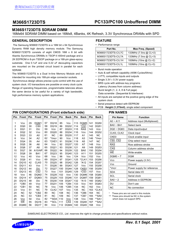
Samsung M366S1723DTS is a 128MB PC133/PC100 unbuffered SDRAM DIMM module built with eight 16Mx8 CMOS synchronous DRAMs in TSOP-II packages and a 2K EEPROM for serial presence detect. Operating at 3.3V with LVTTL-compatible interfaces, it supports 133MHz or 100MHz frequencies with programmable CAS latency of 2 or 3, burst lengths of 1, 2, 4, 8, and full page, and auto/self refresh capability. The 168-pin DIMM module is designed for mounting in standard edge connector sockets, targeting desktop computer memory upgrades and system integrators requiring high-bandwidth synchronous DRAM solutions for mainstream computing applications.
Page 1 Text Content
查询M366S1723DTS供应商
M366S1723DTS PC133/PC100 Unbuffered DIMM
M366S1723DTS SDRAM DIMM 16Mx64 SDRAM DIMM based on 16Mx8, 4Banks, 4K Refresh, 3.3V Synchronous DRAMs with SPD
FEATUREGENERAL DESCRIPTION The Samsung M366S1723DTS is a 16M bit x 64 Synchronous • Performance range
Dynamic RAM high density memory module. The Samsung Part No. Max Freq. (Speed) M366S1723DTS consists of eight CMOS 16M x 8 bit with M366S1723DTS-C/L7C 133MHz (7.5ns @ CL=2) 4banks Synchronous DRAMs in TSOP-II 400mil package and a
M366S1723DTS-C/L7A 133MHz (7.5ns @ CL=3)
2K EEPROM in 8-pin TSSOP package on a 168-pin glass-epoxy
M366S1723DTS-C/L1H 100MHz (10ns @ CL=2)
substrate. One 0.1u F and one 0.22 u F decoupling capacitors
M366S1723DTS-C/L1L 100MHz (10ns @ CL=3)
are mounted on the printed circuit board in parallel for each
• Burst mode operation
SDRAM.
• Auto & self refresh capability (4096 Cycles/64ms)
The M366S1723DTS is a Dual In-line Memory Module and is
• LVTTL compatible inputs and outputs
intended for mounting into 168-pin edge connector sockets.
• Single 3.3V ± 0.3V power supply
Synchronous design allows precise cycle control with the use of
• MRS cycle with address key programs
system clock. I/O transactions are possible on every clock cycle.
Latency (Access from column address)
Range of operating frequencies, programmable latencies allows
Burst length (1, 2, 4, 8 & Full page)
the same device to be useful for a variety of high bandwidth,
Data scramble (Sequential & Interleave)
high performance memory system applications.
• All inputs are sampled at the positive going edge of the system clock • Serial presence detect with EEPROM • PCB : Height (1,375mil), single sided component
PIN CONFIGURATIONS (Front side/back side) PIN NAMES
Pin Pin Pin Pin Pin Pin Pin Name Function
A0 ~ A11 Address input (Multiplexed)
VSS DQM1 DQ18 VSS DQM5 DQ50
BA0 ~ BA1 Select bank
DQ0 CS0 DQ19 DQ32 *CS1 DQ51
DQ1 DU VDD DQ33 RAS VDD DQ0 ~ DQ63 Data input/output
DQ2 VSS DQ20 DQ34 VSS DQ52
CLK0, CLK2 Clock input
DQ3 A0 NC DQ35 A1 NC
CKE0 Clock enable input
VDD A2 *VREF VDD A3 *VREF
CS0, CS2 Chip select input
DQ4 A4 *CKE1 DQ36 A5 NC DQ5 A6 VSS DQ37 A7 VSS RAS Row address strobe DQ6 A8 DQ21 DQ38 A9 DQ53
CAS Column address strobe
DQ7 A10/AP DQ22 DQ39 BA0 DQ54
WE Write enable
DQ8 BA1 DQ23 DQ40 A11 DQ55
VSS VDD VSS VSS VDD VSS DQM0 ~ 7 DQM
DQ9 VDD DQ24 DQ41 *CLK1 DQ56
VDD Power supply (3.3V)
DQ10 CLK0 DQ25 DQ42 *A12 DQ57
VSS Ground
DQ11 VSS DQ26 DQ43 VSS DQ58
DQ12 DU DQ27 DQ44 CKE0 DQ59 *VREF Power supply for reference
DQ13 CS2 VDD DQ45 *CS3 VDD SDA Serial data I/O
VDD DQM2 DQ28 VDD DQM6 DQ60
SCL Serial clock
DQ14 DQM3 DQ29 DQ46 DQM7 DQ61
SA0 ~ 2 Address in EEPROM
DQ15 DU DQ30 DQ47 *A13 DQ62
*CB0 VDD DQ31 *CB4 VDD DQ63 DU Don′t use
*CB1 NC VSS *CB5 NC VSS
NC No connection
VSS NC CLK2 VSS NC *CLK3 NC *CB2 NC NC *CB6 NC * These pins are not used in this module. NC *CB3 NC NC *CB7 **SA0 ** These pins should be NC in the system
VDD VSS **SDA VDD VSS **SA1 which does not support SPD.
WE DQ16 **SCL CAS DQ48 **SA2
DQM0 DQ17 VDD DQM4 DQ49 VDD
SAMSUNG ELECTRONICS CO., Ltd. reserves the right to change products and specifications without notice.
Rev. 0.1 Sept. 2001
Page Summary Contents For Samsung M366S1723DTS datasheet specifications manual user guide
Manual Details
| Brand | Samsung |
|---|---|
| Pages | 11 |
| File Size | 96.26 KB |
| Published | June 16, 2026 |
Enter the captcha to get the download link:

Frequently Asked Questions
What is the operating voltage of M366S1723DTS?
It uses a single 3.3V ± 0.3V power supply.
What is the max frequency of M366S1723DTS-C/L7C?
Its max frequency is 133MHz (7.5ns @ CL=2).
What refresh cycle does this SDRAM DIMM support?
It supports auto & self refresh with 4096 cycles per 64ms.
What socket does M366S1723DTS fit into?
It mounts into 168-pin edge connector sockets.